使用AS6500和ATmega328以激光精度追踪时间
同步起来——时间不等人
已发布 6月 25, 2024
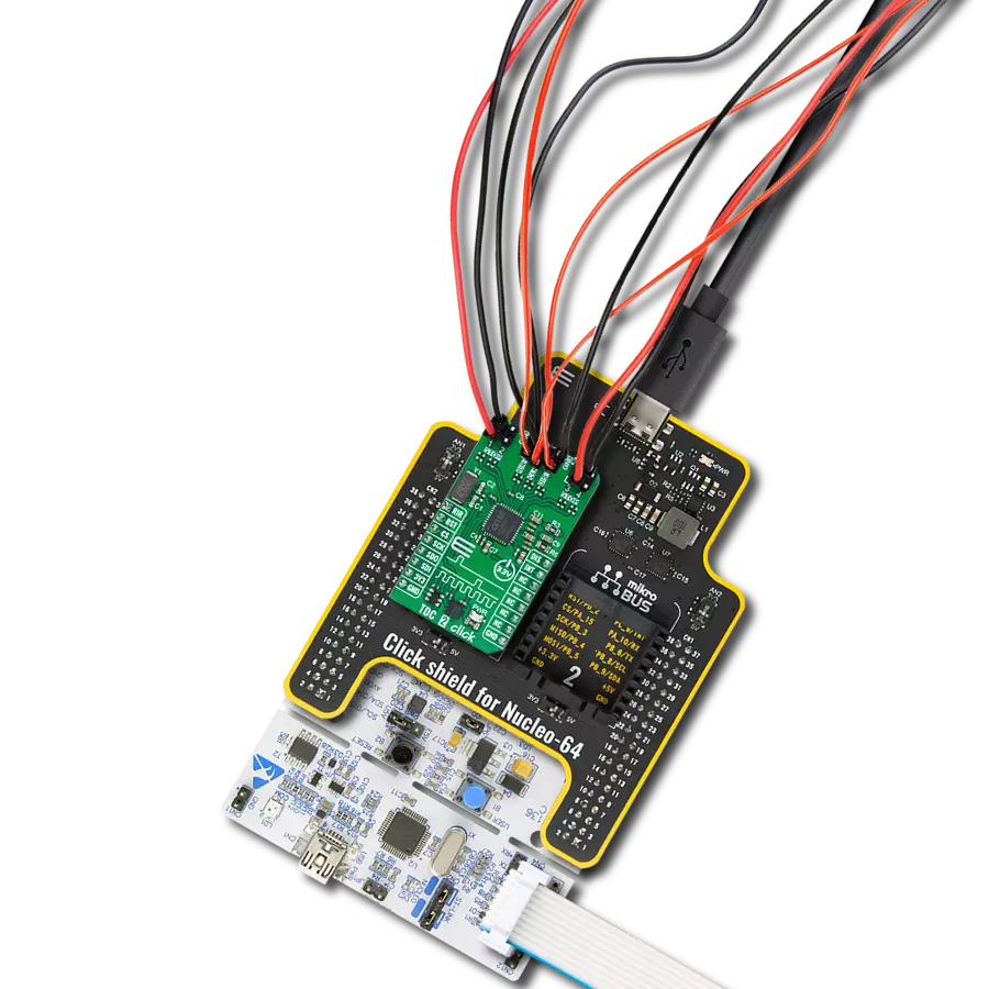
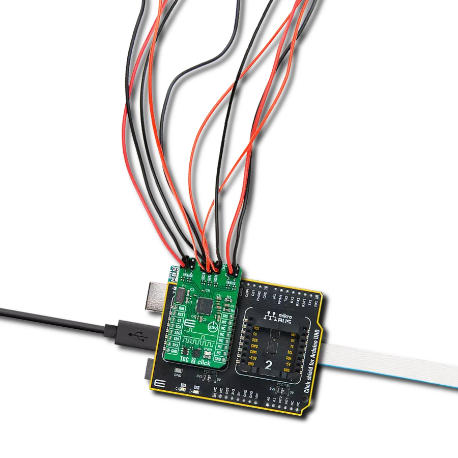
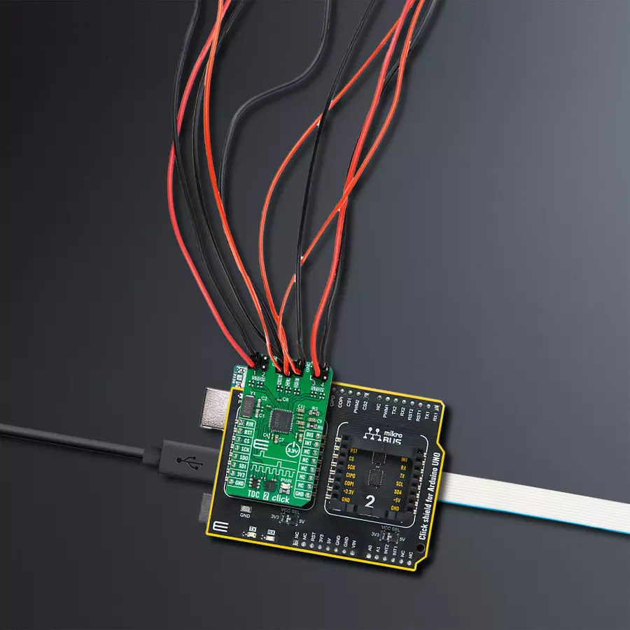
点击板
TDC 2 Click
开发板
Arduino UNO Rev3
编译器
NECTO Studio
微控制器单元
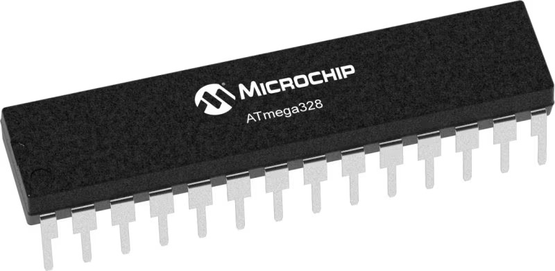
ATmega328
释放这款高性能时间数字转换器的无限可能。
A
A
硬件概览
它是如何工作的?
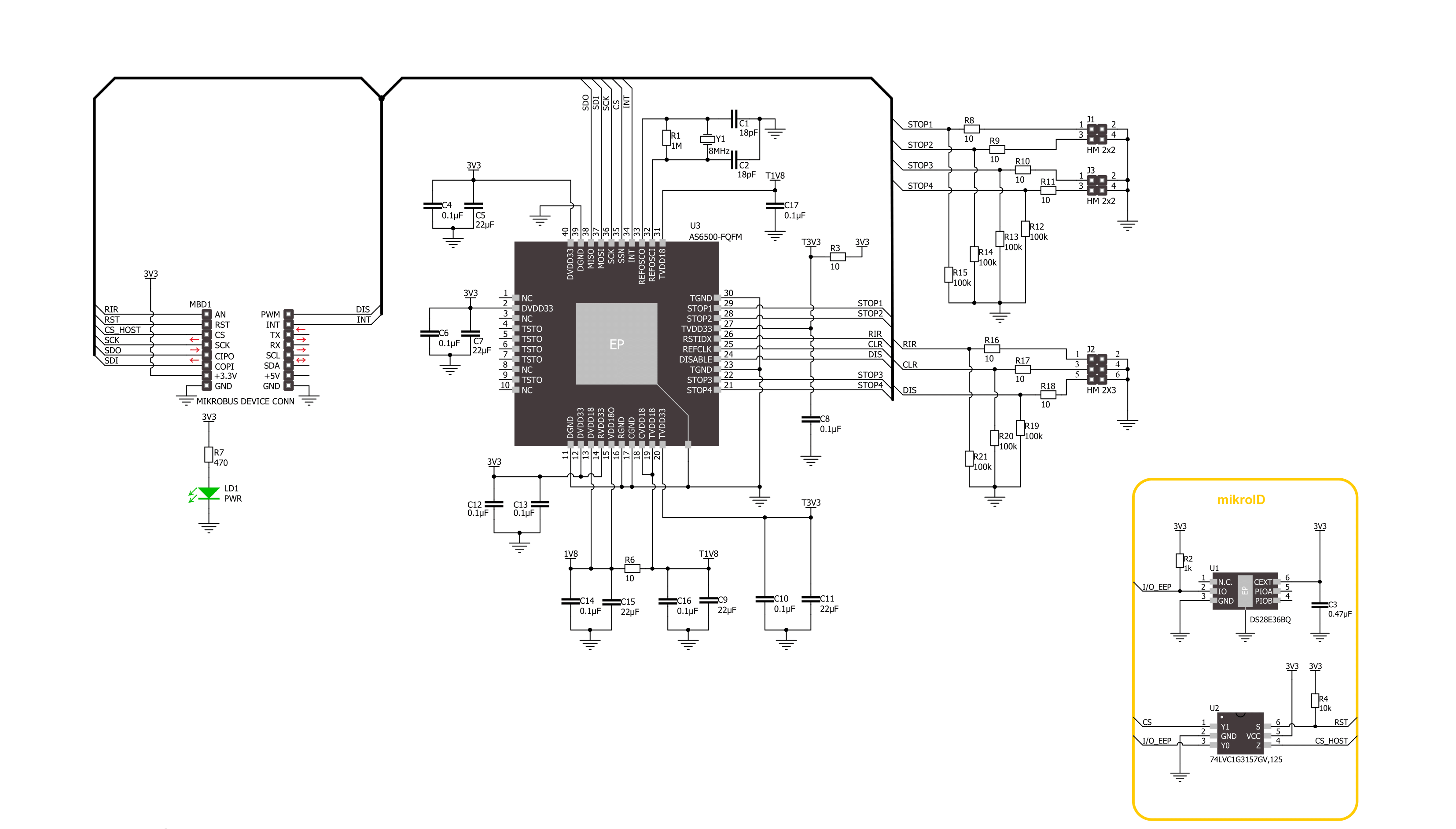
TDC 2 Click 基于 AS6500,这是一款来自 ScioSense 的高分辨率时间数字转换器,具有 CMOS 输入、高测量性能和高数据吞吐量。AS6500 可以在所有四个 STOP 通道上以 10ps 的分辨率测量低至 5ns 的时间间隔,采样率高达 1.5Ms/s。它具有高度的配置灵活性、0 到 16s 的宽测量范围,以及通过校准结果实现的简单数据后处理。它计算相对于应用的参考时钟的校准停止测量。这款 Click board™ 非常适合光学应用,包括一维、二维和三维的通用激光距离测量、速度控制、对象识别、飞行时间光谱等。施加在 STOP 端子(1-4)上的停止信号的正沿相对于前面的参考时钟沿进行测量。参考时钟可以
通过中间端子的 CLR 引脚外部引入,也可以来自板载 8MHz 石英振荡器。此功能可通过软件寄存器设置选择。参考时钟代表所有时间测量的框架,并作为通用时间基准。TDC 连续测量时钟脉冲作为 STOP 脉冲和内部参考周期的时间参考点。STOP 事件的测量始终参考前面的参考时钟。参考时钟连续计数,实际计数作为参考索引分配给 STOP 脉冲。TDC 2 Click 通过标准 SPI 接口与主机 MCU 通信,以读取数据和配置前端,支持高达 50MHz 的高时钟速度和最常见的 SPI 模式,SPI 模式 1。SPI 引脚还使用中断引脚,向主机 MCU 指示数据已准备好处理。AS6500 使用 mikroBUS™ 插座上的几个信号进行成功
的时间测量。使用 RIR 引脚,将参考索引的内部计数器重新设置为零,简化输出数据流中参考索引的概览。接下来,将标记为 DIS 的禁用引脚设置为高逻辑状态,禁用所有四个停止通道的测量。另一方面,参考时钟不受影响,内部参考测量继续。除了 mikroBUS™ 插座外,这些信号还可以在中间接头上找到,与参考时钟引脚分组。此 Click board™ 只能在 3.3V 逻辑电压水平下运行。在使用具有不同逻辑电平的 MCU 之前,板必须进行适当的逻辑电压电平转换。此外,该 Click board™ 配备了包含易于使用的函数和示例代码的库,可作为进一步开发的参考。

功能概述
开发板
Arduino UNO 是围绕 ATmega328P 芯片构建的多功能微控制器板。它为各种项目提供了广泛的连接选项,具有 14 个数字输入/输出引脚,其中六个支持 PWM 输出,以及六个模拟输入。其核心组件包括一个 16MHz 的陶瓷谐振器、一个 USB 连接器、一个电
源插孔、一个 ICSP 头和一个复位按钮,提供了为板 子供电和编程所需的一切。UNO 可以通过 USB 连接到计算机,也可以通过 AC-to-DC 适配器或电池供电。作为第一个 USB Arduino 板,它成为 Arduino 平台的基准,"Uno" 符号化其作为系列首款产品的地
位。这个名称选择,意为意大利语中的 "一",是为了 纪念 Arduino Software(IDE)1.0 的推出。最初与 Arduino Software(IDE)版本1.0 同时推出,Uno 自此成为后续 Arduino 发布的基础模型,体现了该平台的演进。

微控制器概述
MCU卡片 / MCU
建筑
AVR
MCU 内存 (KB)
32
硅供应商
Microchip
引脚数
32
RAM (字节)
2048
你完善了我!
配件
Click Shield for Arduino UNO 具有两个专有的 mikroBUS™ 插座,使所有 Click board™ 设备能够轻松与 Arduino UNO 板进行接口连接。Arduino UNO 是一款基于 ATmega328P 的微控制器开发板,为用户提供了一种经济实惠且灵活的方式来测试新概念并构建基于 ATmega328P 微控制器的原型系统,结合了性能、功耗和功能的多种配置选择。Arduino UNO 具有 14 个数字输入/输出引脚(其中 6 个可用作 PWM 输出)、6 个模拟输入、16 MHz 陶瓷谐振器(CSTCE16M0V53-R0)、USB 接口、电源插座、ICSP 头和复位按钮。大多数 ATmega328P 微控制器的引脚都连接到开发板左右两侧的 IO 引脚,然后再连接到两个 mikroBUS™ 插座。这款 Click Shield 还配备了多个开关,可执行各种功能,例如选择 mikroBUS™ 插座上模拟信号的逻辑电平,以及选择 mikroBUS™ 插座本身的逻辑电压电平。此外,用户还可以通过现有的双向电平转换电压转换器使用任何 Click board™,无论 Click board™ 运行在 3.3V 还是 5V 逻辑电压电平。一旦将 Arduino UNO 板与 Click Shield for Arduino UNO 连接,用户即可访问数百种 Click board™,并兼容 3.3V 或 5V 逻辑电压电平的设备。

使用的MCU引脚
mikroBUS™映射器
“仔细看看!”
Click board™ 原理图
一步一步来
项目组装

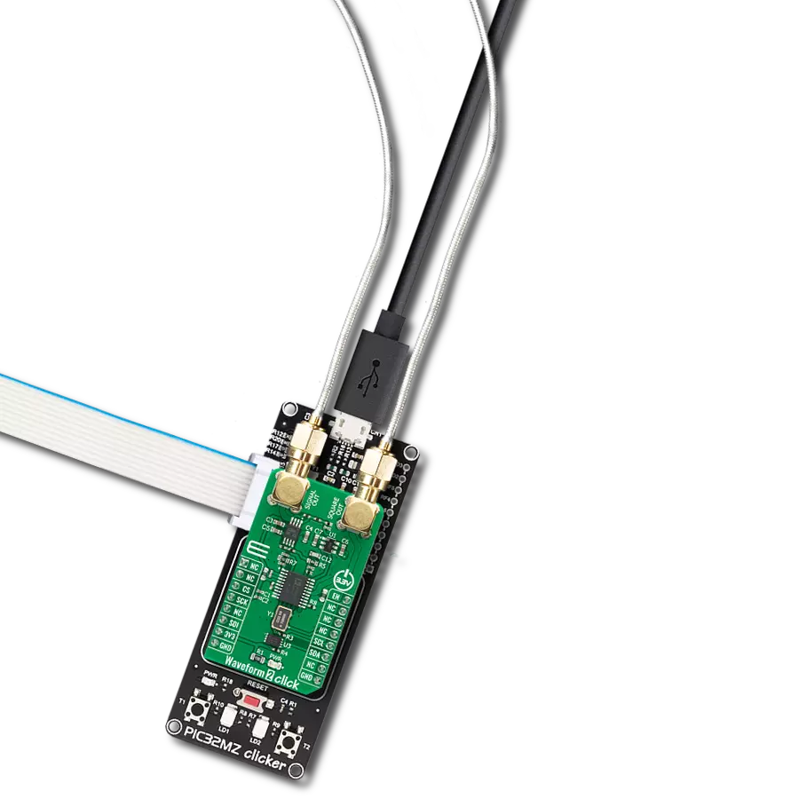
从选择您的开发板和Click板™开始。以Arduino UNO Rev3作为您的开发板开始。


软件支持
库描述
该库包含 TDC 2 Click 驱动程序的 API。
关键功能:
tdc2_read_results- TDC 2 结果数据读取功能tdc2_start_measuring- TDC 2 开始测量功能tdc2_set_resolution- TDC 2 设置分辨率功能
开源
代码示例
完整的应用程序代码和一个现成的项目可以通过NECTO Studio包管理器直接安装到NECTO Studio。 应用程序代码也可以在MIKROE的GitHub账户中找到。
/*!
 * @file main.c
 * @brief TDC 2 Click example
 *
 * # Description
 * This library contains API for TDC 2 Click driver.
 * The library initializes and defines the SPI bus drivers to
 * write and read data from registers, as well as the default
 * configuration for a reading time between two STOP signals.
 *
 * The demo application is composed of two sections :
 *
 * ## Application Init
 * Initializes the driver after that resets the device and
 * performs default configuration and sets the device in read mode.

 *
 * ## Application Task
 * This example demonstrates the use of the TDC 2 Click board by
 * measuring the time between two STOP signals. This example is set up to
 * generate stop signals until FIFO fil's up which is indicated by interrupt pin going to low state.
 * After that FIFO buffer is completely emptied by reading, and that data is used to calculate
 * the time between STOP signals.
 *
 * @note
 * In order to test this example, you will need to connect STOP1 with the DIS pin. Disable pin is
 * disabled by software and it isn't going to affect the working state of the TDC 2 Click Bord.
 *
 * @author Stefan Ilic
 *
 */

#include "board.h"
#include "log.h"
#include "tdc2.h"

static tdc2_t tdc2;
static log_t logger;

/**
 * @brief Dev generate stop signal function.
 * @details This function generates the stop signal by toggling DIS pin.
 * @param[out] cfg : Click configuration structure.
 * See #tdc2_cfg_t object definition for detailed explanation.
 * @return Nothing.
 * @note DIS pin ( Disable STOP channels) is disabled by software and isn't affecting the example.
 */
void dev_generate_stop( tdc2_t *ctx );

void application_init ( void )
{
    log_cfg_t log_cfg;  /**< Logger config object. */
    tdc2_cfg_t tdc2_cfg;  /**< Click config object. */

    /**
     * Logger initialization.
     * Default baud rate: 115200
     * Default log level: LOG_LEVEL_DEBUG
     * @note If USB_UART_RX and USB_UART_TX
     * are defined as HAL_PIN_NC, you will
     * need to define them manually for log to work.
     * See @b LOG_MAP_USB_UART macro definition for detailed explanation.
     */
    LOG_MAP_USB_UART( log_cfg );
    log_init( &logger, &log_cfg );
    log_info( &logger, " Application Init " );

    // Click initialization.
    tdc2_cfg_setup( &tdc2_cfg );
    TDC2_MAP_MIKROBUS( tdc2_cfg, MIKROBUS_1 );
    if ( SPI_MASTER_ERROR == tdc2_init( &tdc2, &tdc2_cfg ) )
    {
        log_error( &logger, " Communication init." );
        for ( ; ; );
    }

    if ( TDC2_ERROR == tdc2_default_cfg ( &tdc2 ) )
    {
        log_error( &logger, " Default configuration." );
        for ( ; ; );
    }

    tdc2_start_measuring ( &tdc2 );
    log_info( &logger, " Application Task " );
}

void application_task ( void )
{
    uint32_t reference_index [ 18 ] = { 0 };
    uint32_t stop_result [ 18 ] = { 0 };
    uint8_t cnt = 0;

    tdc2_reset_index( &tdc2 );
    Delay_ms ( 10 );

    while ( tdc2_get_int_state( &tdc2 ) == 1 )
    {
        dev_generate_stop( &tdc2 );
        Delay_ms ( 100 );
    }

    while ( tdc2_get_int_state( &tdc2 ) == 0 )
    {
        tdc2_read_results( &tdc2, TDC2_REG_INDEX_CH1_BYTE3, &reference_index[ cnt ], &stop_result[ cnt ] );

        log_printf( &logger, "CH1: Reference Index[%d]: %lu, Stop Result[%d]: %lu \r\n", ( uint16_t ) cnt,
                    reference_index[ cnt ], ( uint16_t ) cnt, stop_result[ cnt ] );
        Delay_ms ( 10 );

        if ( cnt )
        {
            uint32_t time = 0;
            tdc2_get_time_between_stops ( &tdc2, stop_result[ cnt - 1 ], reference_index[ cnt - 1 ],
                                          stop_result[ cnt ], reference_index[ cnt ], &time );
            log_printf( &logger, "Time between STOP %d and STOP %d is %lu ms \r\n",
                        ( uint16_t ) ( cnt - 1 ), ( uint16_t ) cnt, time / TDC2_uS_TO_mS );
            Delay_ms ( 10 );
        }
        cnt++;
    }
    log_printf( &logger, "---------------------------------------------- \r\n" );
}

int main ( void )
{
    /* Do not remove this line or clock might not be set correctly. */
    #ifdef PREINIT_SUPPORTED
    preinit();
    #endif

    application_init( );

    for ( ; ; )
    {
        application_task( );
    }

    return 0;
}

void dev_generate_stop( tdc2_t *ctx )
{
    digital_out_high( &ctx->dis );
    Delay_ms ( 1 );
    digital_out_low( &ctx->dis );
}

// ------------------------------------------------------------------------ END
额外支持
资源
类别:时钟发生器