Convert analog signals into precise digital values with ADS1015L and PIC32MX470F512H
Delta-sigma (ΔΣ) 12-bit analog-to-digital converter with an I2C-compatible interface

Published Dec 18, 2024
Click board™
ADC 26 Click
Dev. board
6LoWPAN clicker
Compiler
NECTO Studio
MCU
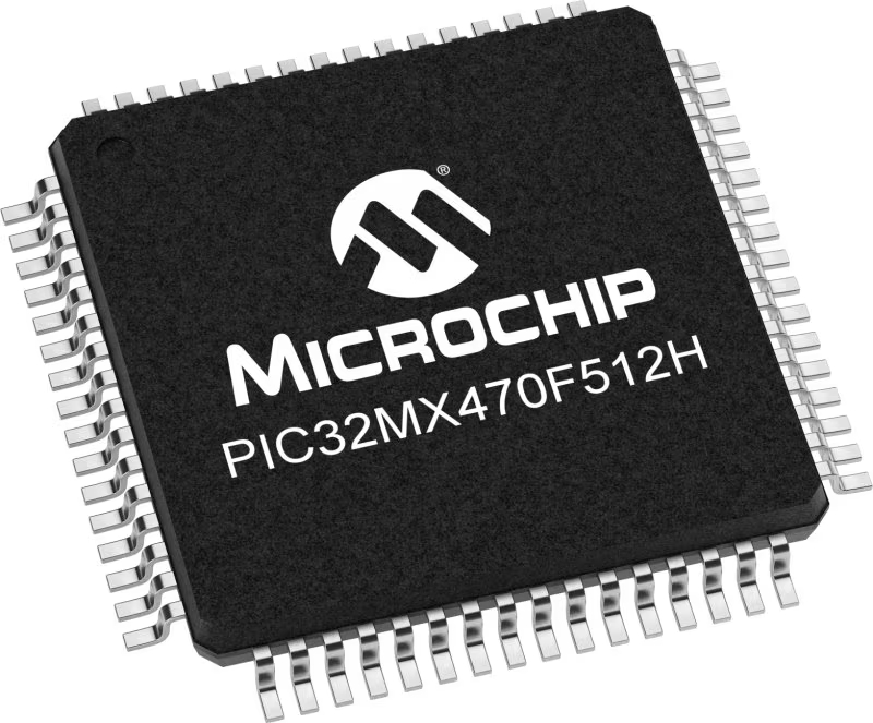
PIC32MX470F512H
Low-power 12-bit analog-to-digital conversion for real-time performance in system monitoring and current sensing
A
A
Hardware Overview
How does it work?
ADC 26 Click is based on the ADS1015L, a low-power 12-bit analog-to-digital converter (ADC) with an I2C-compatible interface from Texas Instruments. It integrates several key components: a ΔΣ ADC core, an internal voltage reference, a clock oscillator, a programmable gain amplifier (PGA), and a programmable digital comparator. This combination enables the ADC to deliver conversions at data rates of up to 3300 samples per second (SPS), making it suitable for applications requiring both high speed and low noise. The ADC core of the ADS1015L measures differential signals brought to its analog input channels (IN0-IN3), offering a flexible full-scale input voltage range from ±0.256V to ±6.144V. This broad range enables the ADS1015L to handle both large and small signals with high precision, making it ideal for general system monitoring tasks such as supply voltage tracking, current sensing, and temperature measurements. These features also cater to applications in wearables and personal electronics. The IC's architecture comprises a differential switched-capacitor ΔΣ modulator followed by a digital filter, ensuring excellent attenuation of common-mode signals and high immunity to noise. The input signal is compared
against the internal voltage reference, while the modulator generates a high-speed bitstream. This stream is processed by the digital filter, which produces a digital output code proportional to the measured voltage. The ADS1015L supports two operational modes designed to optimize power consumption and performance based on application requirements. In single-shot mode, the ADC executes a single measurement upon request, stores the result in an internal register, and then enters a power-down state, making it particularly effective for systems that require periodic measurements or experience extended idle periods between conversions. In continuous-conversion mode, the ADC seamlessly initiates a new measurement as soon as the previous one is completed, maintaining a conversion rate consistent with the configured data rate. This mode is well-suited for real-time monitoring applications, as the data register consistently contains the most recent measurement. This Click board™ is designed in a unique format supporting the newly introduced MIKROE feature called "Click Snap." Unlike the standardized version of Click boards, this feature allows the main IC area to become movable by breaking the PCB, opening up many
new possibilities for implementation. Thanks to the Snap feature, the ADS1015l can operate autonomously by accessing its signals directly on the pins marked 1-8. Additionally, the Snap part includes a specified and fixed screw hole position, enabling users to secure the Snap board in their desired location. ADC 26 Click uses an I2C interface with clock speeds of up to 400kHz, ensuring fast and efficient communication with the host MCU. The I2C address can be easily configured via onboard ADDR SEL jumpers positioned in the Snap part of the board, allowing multiple devices to coexist on the same bus. Additionally, the board features an alert interrupt (AR) pin triggered whenever conversion data exceeds the limit set in the appropriate upper/lower threshold register, or it can be used as a conversion-ready pin. This Click board™ can be operated only with a 3.3V logic voltage level. The board must perform appropriate logic voltage level conversion before using MCUs with different logic levels. It also comes equipped with a library containing functions and example code that can be used as a reference for further development.

Features overview
Development board
6LoWPAN Clicker is a compact starter development board that brings the flexibility of add-on Click boards™ to your favorite microcontroller, making it a perfect starter kit for implementing your ideas. It comes with an onboard 32-bit PIC microcontroller, the PIC32MX470F512H from Microchip, a USB connector, LED indicators, buttons, a mikroProg connector, and a header for interfacing with external electronics. Along with this microcontroller, the board also contains a 2.4GHz ISM band transceiver, allowing you to add wireless communication to your target application. Its compact design provides a fluid and immersive working experience, allowing access anywhere
and under any circumstances. Each part of the 6LoWPAN Clicker development kit contains the components necessary for the most efficient operation of the same board. In addition to the possibility of choosing the 6LoWPAN Clicker programming method, using USB HID mikroBootloader, or through an external mikroProg connector for PIC, dsPIC, or PIC32 programmer, the Clicker board also includes a clean and regulated power supply module for the development kit. The USB Micro-B connection can provide up to 500mA of current for the Clicker board, which is more than enough to operate all onboard and additional modules, or it can power
over two standard AA batteries. All communication methods that mikroBUS™ itself supports are on this board, including the well-established mikroBUS™ socket, reset button, and several buttons and LED indicators. 6LoWPAN Clicker is an integral part of the Mikroe ecosystem, allowing you to create a new application in minutes. Natively supported by Mikroe software tools, it covers many aspects of prototyping thanks to a considerable number of different Click boards™ (over a thousand boards), the number of which is growing every day.

Microcontroller Overview
MCU Card / MCU
Architecture
PIC32
MCU Memory (KB)
512
Silicon Vendor
Microchip
Pin count
64
RAM (Bytes)
131072
Used MCU Pins
mikroBUS™ mapper
Take a closer look
Click board™ Schematic

Step by step
Project assembly

Start by selecting your development board and Click board™. Begin with the 6LoWPAN clicker as your development board.


Software Support
Library Description
This library contains API for ADC 26 Click driver.
Key functions:
adc26_start_conversion- This function starts a single-shot conversion for the selected MUX channel and gain level (full-scale range).adc26_get_alert_pin- This function returns the ALERT (data ready) pin logic state.adc26_read_voltage- This function reads the RAW ADC measurement and converts it to a voltage level.
Open Source
Code example
The complete application code and a ready-to-use project are available through the NECTO Studio Package Manager for direct installation in the NECTO Studio. The application code can also be found on the MIKROE GitHub account.
/*!
 * @file main.c
 * @brief ADC 26 Click example
 *
 * # Description
 * This example demonstrates the use of ADC 26 Click board by reading and
 * displaying the voltage levels from IN0-IN1 differential and IN2-IN3
 * single-ended analog input channels.
 *
 * The demo application is composed of two sections :
 *
 * ## Application Init
 * Initializes the driver and performs the Click default configuration.
 *
 * ## Application Task
 * Reads the voltage levels from IN0-IN1 differential (+/- 2.048V) and
 * IN2-IN3 single-ended (+/- 4.096V) analog input channels and displays
 * the results on the USB UART once per second approximately.
 *
 * @note
 * Do not apply more than VCC + 0.3 V to the analog inputs of the device.
 *
 * @author Stefan Filipovic
 *
 */

#include "board.h"
#include "log.h"
#include "adc26.h"

static adc26_t adc26;
static log_t logger;

void application_init ( void )
{
    log_cfg_t log_cfg;  /**< Logger config object. */
    adc26_cfg_t adc26_cfg;  /**< Click config object. */

    /**
     * Logger initialization.
     * Default baud rate: 115200
     * Default log level: LOG_LEVEL_DEBUG
     * @note If USB_UART_RX and USB_UART_TX
     * are defined as HAL_PIN_NC, you will
     * need to define them manually for log to work.
     * See @b LOG_MAP_USB_UART macro definition for detailed explanation.
     */
    LOG_MAP_USB_UART( log_cfg );
    log_init( &logger, &log_cfg );
    log_info( &logger, " Application Init " );

    // Click initialization.
    adc26_cfg_setup( &adc26_cfg );
    ADC26_MAP_MIKROBUS( adc26_cfg, MIKROBUS_1 );
    if ( I2C_MASTER_ERROR == adc26_init( &adc26, &adc26_cfg ) )
    {
        log_error( &logger, " Communication init." );
        for ( ; ; );
    }

    if ( ADC26_ERROR == adc26_default_cfg ( &adc26 ) )
    {
        log_error( &logger, " Default configuration." );
        for ( ; ; );
    }

    log_info( &logger, " Application Task " );
}

void application_task ( void )
{
    float voltage = 0;
    if ( ADC26_OK == adc26_start_conversion ( &adc26, ADC26_MUX_P_AIN0_N_AIN1, ADC26_PGA_2_048V ) )
    {
        while ( adc26_get_alert_pin ( &adc26 ) ); // Waits for a data ready indication

        if ( ADC26_OK == adc26_read_voltage ( &adc26, &voltage ) )
        {
            log_printf ( &logger, " Voltage between IN0[P] and IN1[N]: %.3f V\r\n", voltage );
        }
    }
    if ( ADC26_OK == adc26_start_conversion ( &adc26, ADC26_MUX_P_AIN2_N_GND, ADC26_PGA_4_096V ) )
    {
        while ( adc26_get_alert_pin ( &adc26 ) ); // Waits for a data ready indication

        if ( ADC26_OK == adc26_read_voltage ( &adc26, &voltage ) )
        {
            log_printf ( &logger, " Voltage between IN2 and GND: %.3f V\r\n", voltage );
        }
    }
    if ( ADC26_OK == adc26_start_conversion ( &adc26, ADC26_MUX_P_AIN3_N_GND, ADC26_PGA_4_096V ) )
    {
        while ( adc26_get_alert_pin ( &adc26 ) ); // Waits for a data ready indication

        if ( ADC26_OK == adc26_read_voltage ( &adc26, &voltage ) )
        {
            log_printf ( &logger, " Voltage between IN3 and GND: %.3f V\r\n\n", voltage );
        }
    }
    Delay_ms ( 1000 );
}

int main ( void )
{
    /* Do not remove this line or clock might not be set correctly. */
    #ifdef PREINIT_SUPPORTED
    preinit();
    #endif

    application_init( );

    for ( ; ; )
    {
        application_task( );
    }

    return 0;
}

// ------------------------------------------------------------------------ END
Additional Support
Resources
Category:ADC


