Provide CAN FD communication with advanced fail-safe mechanisms using ATA6501 and ATmega328
High-speed CAN FD communication solution

Published Feb 03, 2025
Click board™
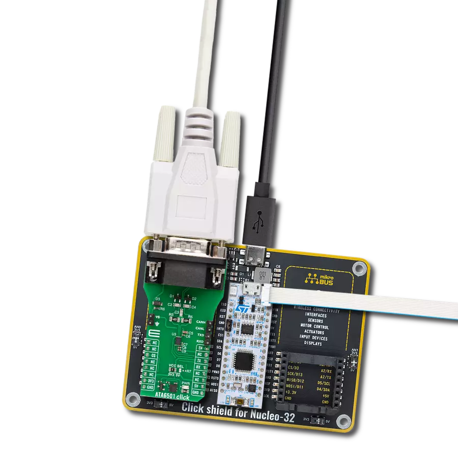
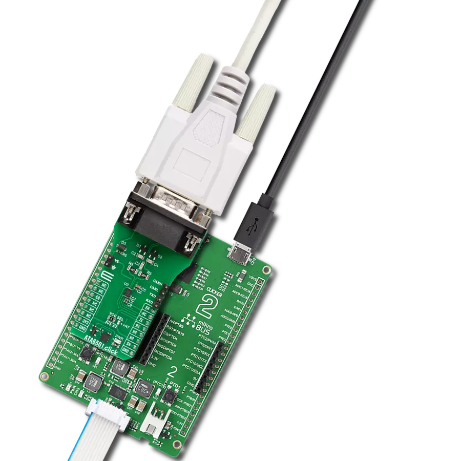
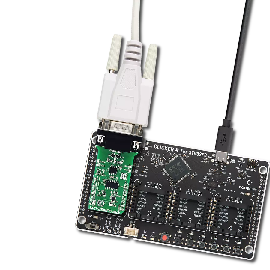
ATA6501 Click
Dev. board
Arduino UNO Rev3
Compiler
NECTO Studio
MCU
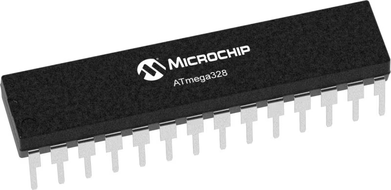
ATmega328
Grade 0 AEC-Q100-qualified classic CAN and CAN FD protocols up to 5Mbit/s
A
A
Hardware Overview
How does it work?
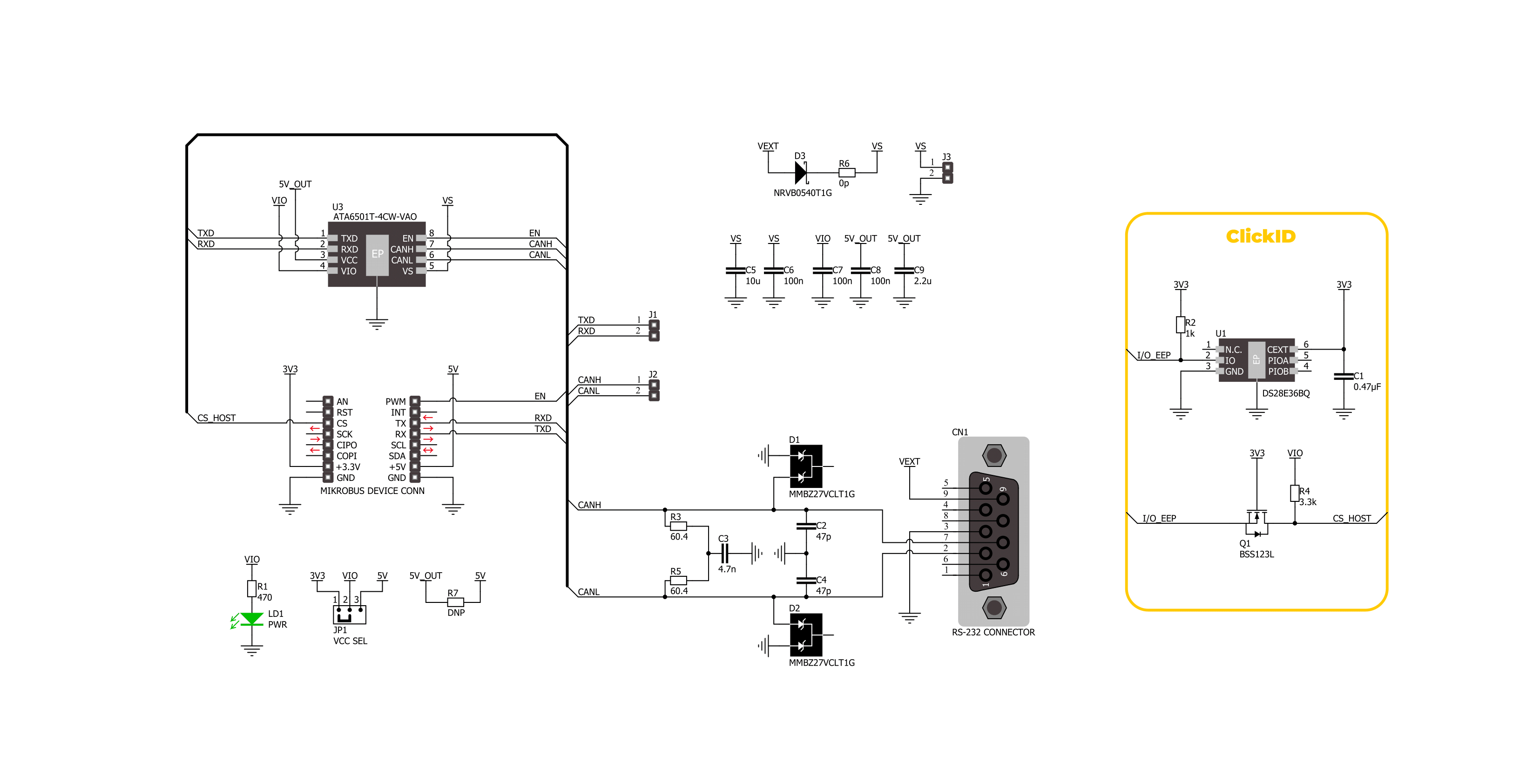
ATA6501 Click is based on the ATA6501, a fully integrated high-speed CAN FD System Basis Chip (SBC) from Microchip. This automotive-qualified device, meeting Grade 0 AEC-Q100 standards, is a reliable interface between a Controller Area Network (CAN) protocol controller and the physical two-wire CAN bus. It supports both Classical CAN and CAN FD communication protocols, achieving data rates of up to 5Mbit/s. Its differential transmit and receive capabilities simplify communication with a CAN protocol controller, enabling the development of reliable CAN nodes. Fully compliant with ISO 11898-2:2024 and SAE J2284-1 to SAE J2284-5 specifications, the ATA6501 ensures compatibility with modern automotive and industrial CAN applications like body electronics and lighting, automotive infotainment systems, powertrain systems, Advanced Driver Assistance Systems (ADAS), photovoltaic systems, and many other scenarios. The ATA6501 communicates with the host MCU through a UART interface, with a default baud rate of 115200bps. This Click board™ features a standard DB-9 connector, allowing straightforward integration with the CAN bus. For added versatility, both CAN and UART signals are
accessible through additional pins on the right side of the Click board™, allowing flexible control options such as monitoring data flow, configuring alternative communication paths, or integrating with auxiliary devices in complex systems. The high-speed CAN FD SBC ATA6501 supports multiple operating modes, advanced diagnostic features, and fail-safe mechanisms, contributing to system reliability and power management. The control pins EN and TXD (connected to the RX pin on the mikroBUS™ socket) select one of the five operating modes provided by the ATA6501 to suit various application requirements. The ATA6501 also features an integrated 5V/150mA voltage regulator capable of powering the CAN FD transceiver, a 5V MCU, and other components or loads on the PCB. In cases where the entire system needs to be powered through the internal 5V regulator, the R7 resistor, left unsoldered by default, must be installed to enable this functionality. The regulator has protection mechanisms for reliable operation under varying conditions, including current limitations and overtemperature shutdown. Additionally, the output voltage is continuously monitored while the regulator is active, and in the
event of an overvoltage condition, the regulator automatically shuts down to prevent potential damage to the system. In addition to the CAN and TXD/RXD pins, the board includes a header with a VS pin, which serves as an external power supply input, supporting a voltage range from 4.5V to 28V. This pin is connected to the power source through a serial diode, providing reverse battery protection and ensuring reliable operation under standard automotive conditions. An integrated undervoltage detection circuit further enhances system reliability by preventing malfunctions or false bus messages caused by insufficient supply voltage. Upon powering the VS pin, the ATA6501 enters Reset mode, which activates the internal voltage regulator. Once the regulated voltage stabilizes, the device transitions to Standby mode, ready for further operation. This Click board™ can operate with either 3.3V or 5V logic voltage levels selected via the VCC SEL jumper. This way, both 3.3V and 5V capable MCUs can use the communication lines properly. Also, this Click board™ comes equipped with a library containing easy-to-use functions and an example code that can be used as a reference for further development.

Features overview
Development board
Arduino UNO is a versatile microcontroller board built around the ATmega328P chip. It offers extensive connectivity options for various projects, featuring 14 digital input/output pins, six of which are PWM-capable, along with six analog inputs. Its core components include a 16MHz ceramic resonator, a USB connection, a power jack, an
ICSP header, and a reset button, providing everything necessary to power and program the board. The Uno is ready to go, whether connected to a computer via USB or powered by an AC-to-DC adapter or battery. As the first USB Arduino board, it serves as the benchmark for the Arduino platform, with "Uno" symbolizing its status as the
first in a series. This name choice, meaning "one" in Italian, commemorates the launch of Arduino Software (IDE) 1.0. Initially introduced alongside version 1.0 of the Arduino Software (IDE), the Uno has since become the foundational model for subsequent Arduino releases, embodying the platform's evolution.

Microcontroller Overview
MCU Card / MCU
Architecture
AVR
MCU Memory (KB)
32
Silicon Vendor
Microchip
Pin count
32
RAM (Bytes)
2048
You complete me!
Accessories
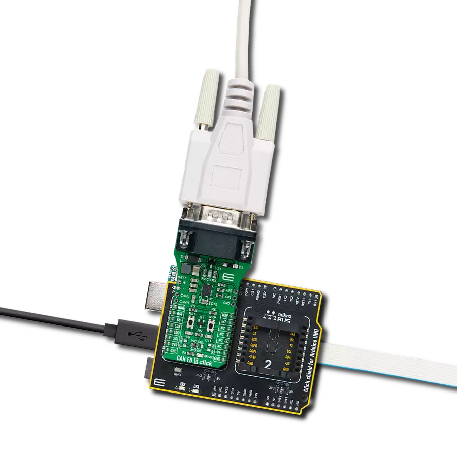
Click Shield for Arduino UNO has two proprietary mikroBUS™ sockets, allowing all the Click board™ devices to be interfaced with the Arduino UNO board without effort. The Arduino Uno, a microcontroller board based on the ATmega328P, provides an affordable and flexible way for users to try out new concepts and build prototypes with the ATmega328P microcontroller from various combinations of performance, power consumption, and features. The Arduino Uno has 14 digital input/output pins (of which six can be used as PWM outputs), six analog inputs, a 16 MHz ceramic resonator (CSTCE16M0V53-R0), a USB connection, a power jack, an ICSP header, and reset button. Most of the ATmega328P microcontroller pins are brought to the IO pins on the left and right edge of the board, which are then connected to two existing mikroBUS™ sockets. This Click Shield also has several switches that perform functions such as selecting the logic levels of analog signals on mikroBUS™ sockets and selecting logic voltage levels of the mikroBUS™ sockets themselves. Besides, the user is offered the possibility of using any Click board™ with the help of existing bidirectional level-shifting voltage translators, regardless of whether the Click board™ operates at a 3.3V or 5V logic voltage level. Once you connect the Arduino UNO board with our Click Shield for Arduino UNO, you can access hundreds of Click boards™, working with 3.3V or 5V logic voltage levels.

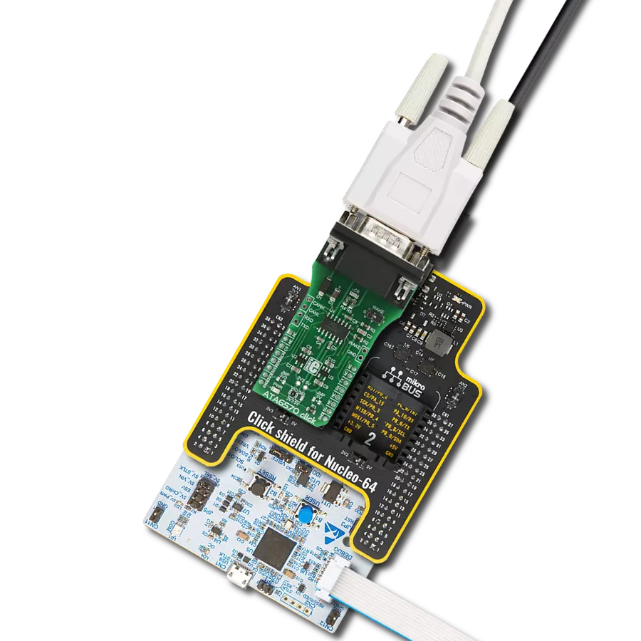
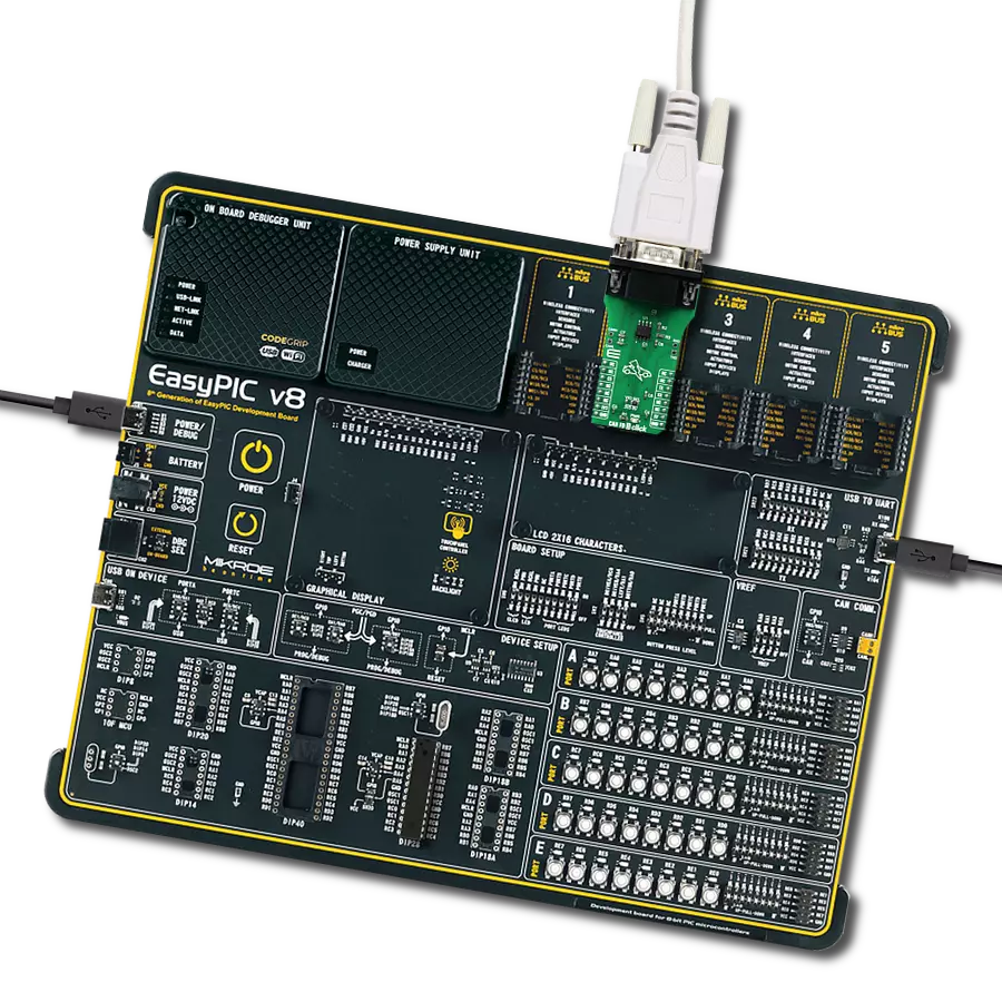
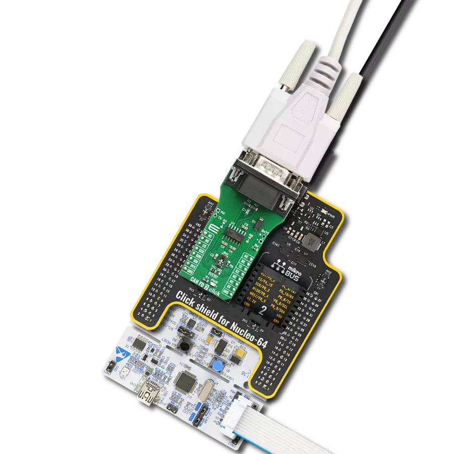
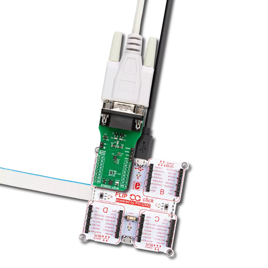
DB9 Cable Female-to-Female (2m) cable is essential for establishing dependable serial data connections between devices. With its DB9 female connectors on both ends, this cable enables a seamless link between various equipment, such as computers, routers, switches, and other serial devices. Measuring 2 meters in length, it offers flexibility in arranging your setup without compromising data transmission quality. Crafted with precision, this cable ensures consistent and reliable data exchange, making it suitable for industrial applications, office environments, and home setups. Whether configuring networking equipment, accessing console ports, or utilizing serial peripherals, this cable's durable construction and robust connectors guarantee a stable connection. Simplify your data communication needs with the 2m DB9 female-to-female cable, an efficient solution designed to meet your serial connectivity requirements easily and efficiently.

Used MCU Pins
mikroBUS™ mapper
Take a closer look
Click board™ Schematic
Step by step
Project assembly

Start by selecting your development board and Click board™. Begin with the Arduino UNO Rev3 as your development board.


Software Support
Library Description
ATA6501 Click demo application is developed using the NECTO Studio, ensuring compatibility with mikroSDK's open-source libraries and tools. Designed for plug-and-play implementation and testing, the demo is fully compatible with all development, starter, and mikromedia boards featuring a mikroBUS™ socket.
Example Description
This example demonstrates the use of an ATA6501 Click board by showing the communication between the two Click boards.
Key functions:
ata6501_cfg_setup- Config Object Initialization function.ata6501_init- Initialization function.ata6501_generic_write- This function writes a desired number of data bytes by using UART serial interface.ata6501_generic_read- This function reads a desired number of data bytes by using UART serial interface.ata6501_set_en_pin- This function sets the EN pin logic state.
Application Init
Initializes the driver and logger.
Application Task
Depending on the selected application mode, it reads all the received data or sends the desired message every 3 seconds.
Open Source
Code example
The complete application code and a ready-to-use project are available through the NECTO Studio Package Manager for direct installation in the NECTO Studio. The application code can also be found on the MIKROE GitHub account.
/*!
 * @file main.c
 * @brief ATA6501 Click Example.
 *
 * # Description
 * This example demonstrates the use of an ATA6501 Click board by showing
 * the communication between the two Click boards.
 *
 * The demo application is composed of two sections :
 *
 * ## Application Init
 * Initializes the driver and logger.
 *
 * ## Application Task
 * Depending on the selected application mode, it reads all the received data or
 * sends the desired message every 3 seconds.
 *
 * ## Additional Function
 * - static void ata6501_clear_app_buf ( void )
 * - static void ata6501_log_app_buf ( void )
 * - static err_t ata6501_process ( ata6501_t *ctx )
 *
 * @author Stefan Filipovic
 *
 */

#include "board.h"
#include "log.h"
#include "ata6501.h"

// Comment out the line below in order to switch the application mode to receiver
#define DEMO_APP_TRANSMITTER

// Text message to send in the transmitter application mode
#define DEMO_TEXT_MESSAGE           "MIKROE - ATA6501 Click board\r\n"

// Application buffer size
#define APP_BUFFER_SIZE             500
#define PROCESS_BUFFER_SIZE         200

static ata6501_t ata6501;
static log_t logger;

static uint8_t app_buf[ APP_BUFFER_SIZE ] = { 0 };
static int32_t app_buf_len = 0;

/**
 * @brief ATA6501 clearing application buffer.
 * @details This function clears memory of application buffer and reset its length.
 * @note None.
 */
static void ata6501_clear_app_buf ( void );

/**
 * @brief ATA6501 log application buffer.
 * @details This function logs data from application buffer to USB UART.
 * @note None.
 */
static void ata6501_log_app_buf ( void );

/**
 * @brief ATA6501 data reading function.
 * @details This function reads data from device and concatenates data to application buffer.
 * @param[in] ctx : Click context object.
 * See #ata6501_t object definition for detailed explanation.
 * @return @li @c  0 - Read some data.
 *         @li @c -1 - Nothing is read.
 * See #err_t definition for detailed explanation.
 * @note None.
 */
static err_t ata6501_process ( ata6501_t *ctx );

void application_init ( void )
{
    log_cfg_t log_cfg;  /**< Logger config object. */
    ata6501_cfg_t ata6501_cfg;  /**< Click config object. */

    /**
     * Logger initialization.
     * Default baud rate: 115200
     * Default log level: LOG_LEVEL_DEBUG
     * @note If USB_UART_RX and USB_UART_TX
     * are defined as HAL_PIN_NC, you will
     * need to define them manually for log to work.
     * See @b LOG_MAP_USB_UART macro definition for detailed explanation.
     */
    LOG_MAP_USB_UART( log_cfg );
    log_init( &logger, &log_cfg );
    log_info( &logger, " Application Init " );

    // Click initialization.
    ata6501_cfg_setup( &ata6501_cfg );
    ATA6501_MAP_MIKROBUS( ata6501_cfg, MIKROBUS_1 );
    if ( UART_ERROR == ata6501_init( &ata6501, &ata6501_cfg ) )
    {
        log_error( &logger, " Communication init." );
        for ( ; ; );
    }

#ifdef DEMO_APP_TRANSMITTER
    log_printf( &logger, " Application Mode: Transmitter\r\n" );
#else
    log_printf( &logger, " Application Mode: Receiver\r\n" );
#endif

    log_info( &logger, " Application Task " );
}

void application_task ( void )
{
#ifdef DEMO_APP_TRANSMITTER
    ata6501_generic_write( &ata6501, DEMO_TEXT_MESSAGE, strlen( DEMO_TEXT_MESSAGE ) );
    log_printf( &logger, "%s", ( char * ) DEMO_TEXT_MESSAGE );
    Delay_ms ( 1000 );
    Delay_ms ( 1000 );
    Delay_ms ( 1000 );
#else
    if ( ATA6501_OK == ata6501_process( &ata6501 ) )
    {
        ata6501_log_app_buf ( );
        ata6501_clear_app_buf ( );
    }
#endif
}

int main ( void )
{
    /* Do not remove this line or clock might not be set correctly. */
    #ifdef PREINIT_SUPPORTED
    preinit();
    #endif

    application_init( );

    for ( ; ; )
    {
        application_task( );
    }

    return 0;
}

static void ata6501_clear_app_buf ( void )
{
    memset( app_buf, 0, app_buf_len );
    app_buf_len = 0;
}

static void ata6501_log_app_buf ( void )
{
    for ( int32_t buf_cnt = 0; buf_cnt < app_buf_len; buf_cnt++ )
    {
        log_printf( &logger, "%c", app_buf[ buf_cnt ] );
    }
}

static err_t ata6501_process ( ata6501_t *ctx )
{
    uint8_t rx_buf[ PROCESS_BUFFER_SIZE ] = { 0 };
    int32_t overflow_bytes = 0;
    int32_t rx_cnt = 0;
    int32_t rx_size = ata6501_generic_read( ctx, rx_buf, PROCESS_BUFFER_SIZE );
    if ( ( rx_size > 0 ) && ( rx_size <= APP_BUFFER_SIZE ) )
    {
        if ( ( app_buf_len + rx_size ) > APP_BUFFER_SIZE )
        {
            overflow_bytes = ( app_buf_len + rx_size ) - APP_BUFFER_SIZE;
            app_buf_len = APP_BUFFER_SIZE - rx_size;
            memmove ( app_buf, &app_buf[ overflow_bytes ], app_buf_len );
            memset ( &app_buf[ app_buf_len ], 0, overflow_bytes );
        }
        for ( rx_cnt = 0; rx_cnt < rx_size; rx_cnt++ )
        {
            if ( rx_buf[ rx_cnt ] )
            {
                app_buf[ app_buf_len++ ] = rx_buf[ rx_cnt ];
            }
        }
        return ATA6501_OK;
    }
    return ATA6501_ERROR;
}

// ------------------------------------------------------------------------ END
Additional Support
Resources
Category:CAN