Connect and control various types of sensors and actuators with AD74115H, ADP1034 and TM4C1294NCZAD
From analog signals to digital commands: AD-SWIO shapes your control

Published Dec 18, 2023
Click board™
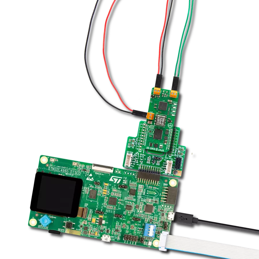
AD-SWIO 3 Click
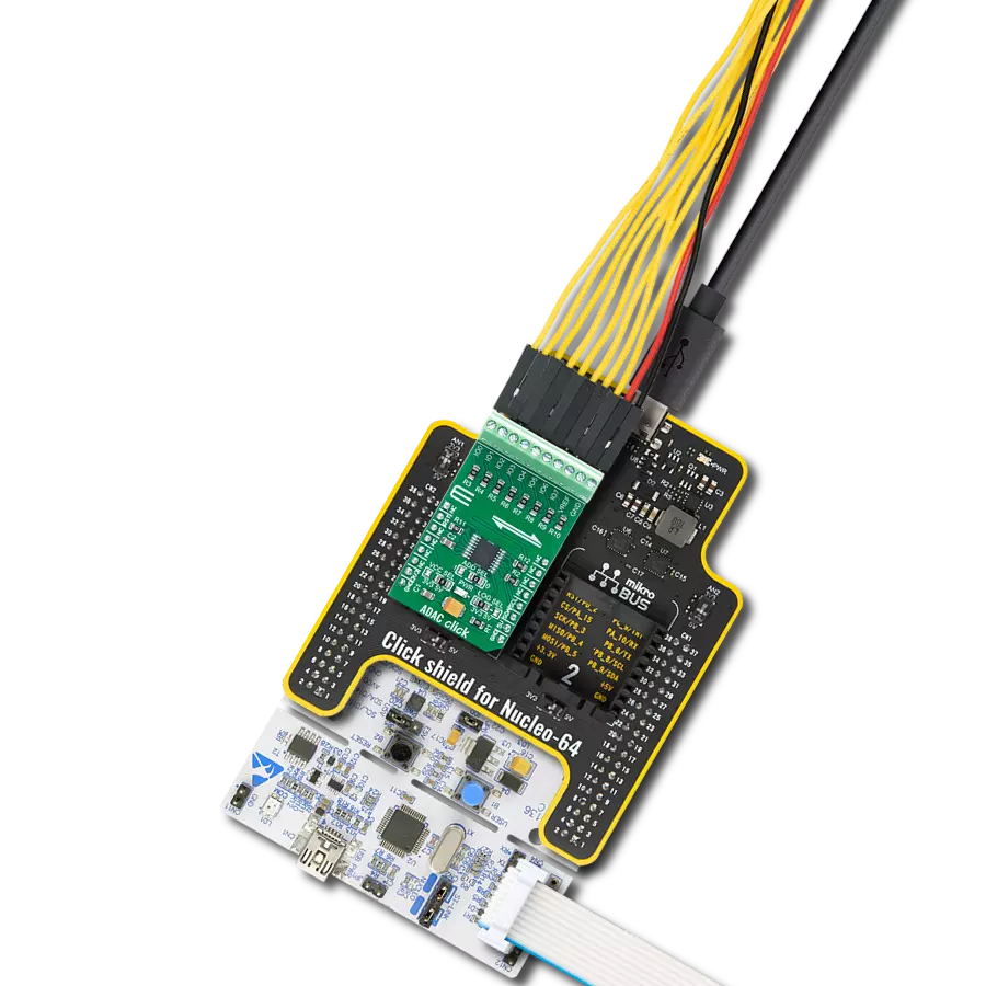
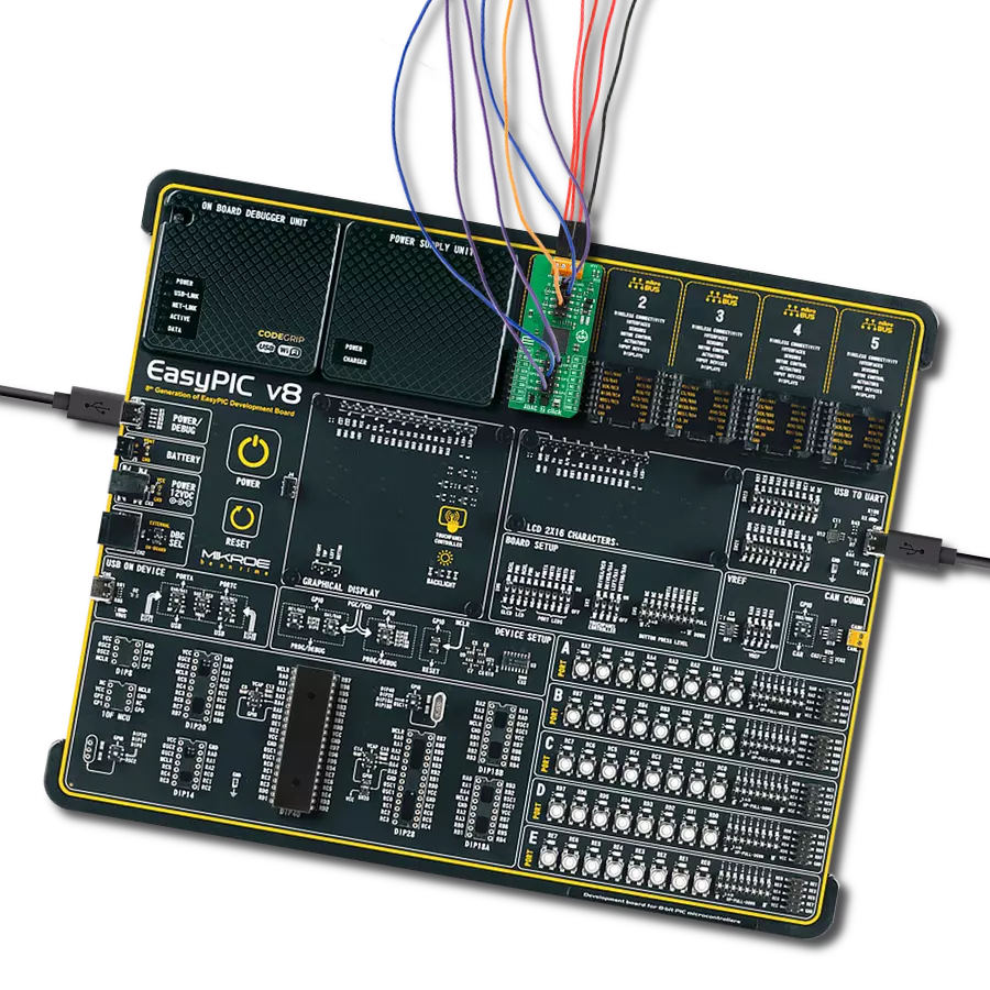
Dev. board
UNI-DS v8
Compiler
NECTO Studio
MCU
TM4C1294NCZAD
Manage and control different devices in industrial and automation setups, ensuring safety and flexibility in the process
A
A
Hardware Overview
How does it work?
AD-SWIO 3 Click is based on the AD74115H, a single-channel, software-configurable input and output with HART mode, and ADP1034, a 3-channel isolated micropower management unit with seven digital isolators and programmable power control both from Analog Devices. The AD74115H has a single-channel input and output, which can be configured as voltage input, current input, voltage output, current output, digital input, digital output, 2/3/4-wire RTD measurement, or thermocouple measurement input. It features a 16-bit, Σ-Δ analog-to-digital converter (ADC) and a 14-bit digital-to-analog converter (DAC), with a high accuracy 2.5V on-chip reference that can be used both for ADC and DAC. You can connect the desired load to terminals labeled I/OP and I/ON for analog output, analog input, and digital input functions. To apply a stimulus to the two auxiliary high-voltage sense pins, use I/O EXT1 and I/O
EXT2 terminals. The resistance measurements can be made between those four terminals, depending on the number of wires RTD. For instance, take 2-wire resistance measurements between the I/OP and I/ON terminals. The integrated HART modem can transmit and receive signals to and from the I/OP terminal. For more info, check the datasheet. Four LEDs (GPIOA, GPIOB, GPIOC, GPIOD) can be configured in several ways to represent digital input, digital output, external or internal conditions, and more. An onboard thermistor is connected to the AD74115H, which can measure the board's temperature. The ADP1034 provides power and isolation to the AD74115H. A flyback regulator supply voltage of 24V can be applied over the VINP terminal. You can control the flyback regulator slew rate over the SLEW jumper between the slowest and normal as default. You can also choose the highest by leaving the SLEW pin open. The
ZA9644-AED, a flyback transformer from Coilcraft, is used for flyback regulator operation. AD-SWIO 3 Click uses a standard 4-wire SPI serial interface of the AD74115H through the isolation that provides the ADP1034 to communicate with the host MCU. You can reset the AD74115H over the RST pin. When a new sequence of ADC conversion is ready to be read, the RDY will be asserted. Also, the alert ALR pin will be asserted when the alert condition is met. All those lines pass through an isolation barrier of the ADP1034 on its way to the host MCU. This Click board™ can be operated only with a 3.3V logic voltage level. The board must perform appropriate logic voltage level conversion before using MCUs with different logic levels. Also, this Click board™ comes equipped with a library containing easy-to-use functions and an example code that can be used for further development.

Features overview
Development board
UNI-DS v8 is a development board specially designed for the needs of rapid development of embedded applications. It supports a wide range of microcontrollers, such as different STM32, Kinetis, TIVA, CEC, MSP, PIC, dsPIC, PIC32, and AVR MCUs regardless of their number of pins, and a broad set of unique functions, such as the first-ever embedded debugger/programmer over WiFi. The development board is well organized and designed so that the end-user has all the necessary elements, such as switches, buttons, indicators, connectors, and others, in one place. Thanks to innovative manufacturing technology, UNI-DS v8 provides a fluid and immersive working experience, allowing access anywhere and under any
circumstances at any time. Each part of the UNI-DS v8 development board contains the components necessary for the most efficient operation of the same board. An advanced integrated CODEGRIP programmer/debugger module offers many valuable programming/debugging options, including support for JTAG, SWD, and SWO Trace (Single Wire Output)), and seamless integration with the Mikroe software environment. Besides, it also includes a clean and regulated power supply module for the development board. It can use a wide range of external power sources, including a battery, an external 12V power supply, and a power source via the USB Type-C (USB-C) connector. Communication options such as USB-UART, USB
HOST/DEVICE, CAN (on the MCU card, if supported), and Ethernet is also included. In addition, it also has the well-established mikroBUS™ standard, a standardized socket for the MCU card (SiBRAIN standard), and two display options for the TFT board line of products and character-based LCD. UNI-DS v8 is an integral part of the Mikroe ecosystem for rapid development. Natively supported by Mikroe software tools, it covers many aspects of prototyping and development thanks to a considerable number of different Click boards™ (over a thousand boards), the number of which is growing every day.

Microcontroller Overview
MCU Card / MCU
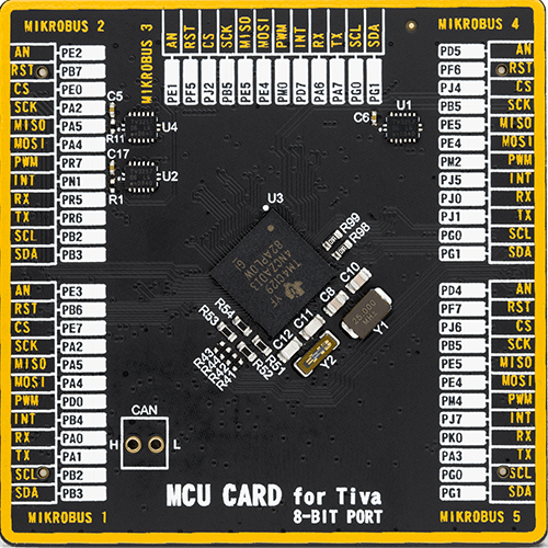
Type
8th Generation
Architecture
ARM Cortex-M4
MCU Memory (KB)
1024
Silicon Vendor
Texas Instruments
Pin count
212
RAM (Bytes)
262144
Used MCU Pins
mikroBUS™ mapper
Take a closer look
Click board™ Schematic

Step by step
Project assembly

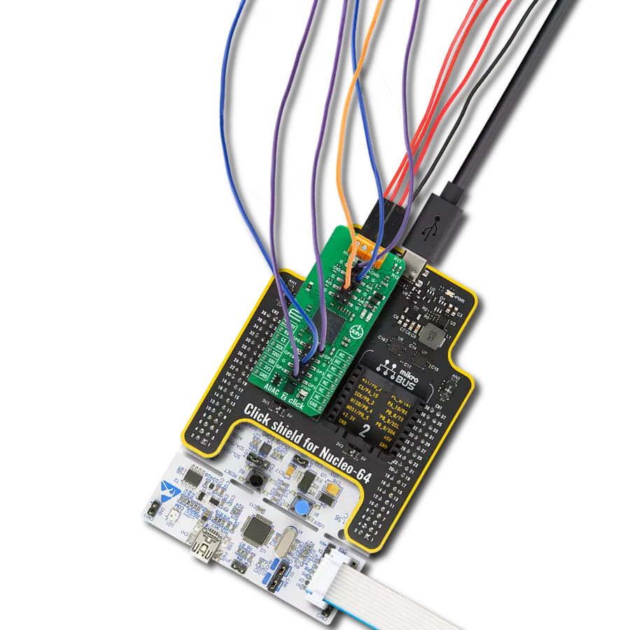
Start by selecting your development board and Click board™. Begin with the UNI-DS v8 as your development board.


Software Support
Library Description
This library contains API for AD-SWIO 3 Click driver.
Key functions:
adswio3_get_voltage_input- This function reads the raw ADC value and converts them to a proportional voltage level measured by the voltage between the I/OP and I/ON screw terminals.adswio3_get_diag_res- This function is used to read the desired diagnostic conversion results.adswio3_set_adc_cnv- This function is used to control the ADC conversions that must be performed.
Open Source
Code example
The complete application code and a ready-to-use project are available through the NECTO Studio Package Manager for direct installation in the NECTO Studio. The application code can also be found on the MIKROE GitHub account.
/*!
 * @file main.c
 * @brief AD-SWIO 3 Click example
 *
 * # Description
 * This library contains API for the AD-SWIO 3 Click driver
 * for measurements of the analog output, analog input, digital input,
 * resistance temperature detector (RTD), and thermocouple measurements.
 *
 * The demo application is composed of two sections :
 *
 * ## Application Init
 * Initialization of SPI and log UART.
 * After driver initialization, the app executes a default configuration
 * that enables and sets it to measure IOP/ION voltage input from 0V to 12V,
 * with 4.8k SPS and enabled four diagnostics measurements (AVDD, VASS, VACC and LVIN).
 *
 * ## Application Task
 * This example demonstrates the use of the AD-SWIO 3 Click board.
 * The demo application reads and displays the voltage level input,
 * measured by the voltage between the I/OP and I/ON screw terminals
 * and NTC thermistor temperature in degrees Celsius.
 * Results are being sent to the UART Terminal, where you can track their changes.
 *
 * @author Nenad Filipovic
 *
 */

#include "board.h"
#include "log.h"
#include "adswio3.h"

static adswio3_t adswio3;
static log_t logger;

void application_init ( void )
{
    log_cfg_t log_cfg;  /**< Logger config object. */
    adswio3_cfg_t adswio3_cfg;  /**< Click config object. */

    /**
     * Logger initialization.
     * Default baud rate: 115200
     * Default log level: LOG_LEVEL_DEBUG
     * @note If USB_UART_RX and USB_UART_TX
     * are defined as HAL_PIN_NC, you will
     * need to define them manually for log to work.
     * See @b LOG_MAP_USB_UART macro definition for detailed explanation.
     */
    LOG_MAP_USB_UART( log_cfg );
    log_init( &logger, &log_cfg );
    log_info( &logger, " Application Init " );

    // Click initialization.
    adswio3_cfg_setup( &adswio3_cfg );
    ADSWIO3_MAP_MIKROBUS( adswio3_cfg, MIKROBUS_1 );
    if ( SPI_MASTER_ERROR == adswio3_init( &adswio3, &adswio3_cfg ) )
    {
        log_error( &logger, " Communication init." );
        for ( ; ; );
    }

    if ( ADSWIO3_ERROR == adswio3_default_cfg ( &adswio3 ) )
    {
        log_error( &logger, " Default configuration." );
        for ( ; ; );
    }
    Delay_ms ( 100 );

    for ( uint8_t n_cnt = ADSWIO3_GPIO_CONFIG_SEL_A; n_cnt <= ADSWIO3_GPIO_CONFIG_SEL_D; n_cnt ++ )
    {
        if ( ADSWIO3_ERROR == adswio3_set_gpio_config( &adswio3, n_cnt,
                                                              ADSWIO3_GPIO_CONFIG_GPO_DATA_HIGH,
                                                              ADSWIO3_GPIO_CONFIG_GP_WK_PD_DIS,
                                                              ADSWIO3_GPIO_CONFIG_MODE_OUT ) )
        {
            log_error( &logger, " Set GPIO configuration. " );
            for ( ; ; );
        }
        Delay_ms ( 100 );
    }

    float diag_vtg = 0;
    log_printf( &logger, "_________________________\r\n" );
    log_printf( &logger, " > Diagnostic Voltages <\r\n" );
    if ( ADSWIO3_OK == adswio3_get_diag_vtg( &adswio3, ADSWIO3_DIAG_RESULT_SEL_0, &diag_vtg ) )
    {
        log_printf( &logger, " AVDD: %.2f V\r\n", diag_vtg );
        Delay_ms ( 100 );
    }

    if ( ADSWIO3_OK == adswio3_get_diag_vtg( &adswio3, ADSWIO3_DIAG_RESULT_SEL_1, &diag_vtg ) )
    {
        log_printf( &logger, " VASS: %.2f V\r\n", diag_vtg );
        Delay_ms ( 100 );
    }

    if ( ADSWIO3_OK == adswio3_get_diag_vtg( &adswio3, ADSWIO3_DIAG_RESULT_SEL_2, &diag_vtg ) )
    {
        log_printf( &logger, " VACC: %.2f V\r\n", diag_vtg );
        Delay_ms ( 100 );
    }

    if ( ADSWIO3_OK == adswio3_get_diag_vtg( &adswio3, ADSWIO3_DIAG_RESULT_SEL_3, &diag_vtg ) )
    {
        log_printf( &logger, " LVIN: %.2f V\r\n", diag_vtg );
        Delay_ms ( 100 );
    }
    log_printf( &logger, "_________________________\r\n" );
    Delay_ms ( 1000 );
}

void application_task ( void )
{
    float ntc_temp = 0, iop_ion_vtg = 0;
    if ( ADSWIO3_OK == adswio3_get_ntc_temp( &adswio3, ADSWIO3_DIAG_RESULT_SEL_3, &ntc_temp ) )
    {
        log_printf( &logger, " NTC Temperature: %.2f degC\r\n", ntc_temp );

        Delay_ms ( 100 );
    }

    if ( ADSWIO3_OK == adswio3_get_voltage_input( &adswio3, 0, &iop_ion_vtg ) )
    {
        log_printf( &logger, "IOP/ION Voltage: %.3f V\r\n", iop_ion_vtg );
        Delay_ms ( 100 );
    }
    log_printf( &logger, "_________________________\r\n" );
    Delay_ms ( 1000 );
}

int main ( void )
{
    /* Do not remove this line or clock might not be set correctly. */
    #ifdef PREINIT_SUPPORTED
    preinit();
    #endif

    application_init( );

    for ( ; ; )
    {
        application_task( );
    }

    return 0;
}

// ------------------------------------------------------------------------ END