Experience the seamless blend of capacity and velocity with AT25SF321B and TM4C129ENCPDT
Flash forward: Upgrade storage, empower innovation

Published Nov 11, 2023
Click board™
Flash 11 Click
Dev. board
Fusion for Tiva v8
Compiler
NECTO Studio
MCU
TM4C129ENCPDT
Data management reaches new heights with our flash memory marvel.
A
A
Hardware Overview
How does it work?
Flash 11 Click is based on the AT25SF321B, a 32-Mbit SPI serial Flash memory with Dual I/O and Quad I/O support from Dialog Semiconductor. The AT25SF321A is organized as a 32Mbit (4Mx8 physical block) Flash memory where the memory array can be erased in four levels of granularity, including a full-chip erase, which, depending on the blocks, can be done typically in 10 seconds. In addition, the optimized erase architecture allows erasing data in 4kB, 32kB, and 64kB block erase operations. Optimizing the erase blocks' size can be the most efficient use of memory space. The AT25SF321B specifies a minimum of 100.000 endurance cycles with data retention of a minimum of 20 years, allowing it to handle (almost) unlimited reads/writes to the memory. Flash 11 Click communicates with MCU through a
standard SPI interface supporting the two most common SPI modes, SPI Mode 0 and 3, and a maximum clock frequency of up to 108MHz. Furthermore, this Click board™ provides additional hardware-controlled functions. The configurable Write Protection, marked as WP and routed on the default position of the PWM pin of the mikroBUS™ socket, protects all registers (including status and configuration) from write operations and must be held low to inhibit all the write operations to registers. When this pin is in a low logic state, all memory and register write are prohibited, and the address count is not incremented. In addition, there is software write protection too. Also, it is possible to use the Reset or Hold function through the RST pin of the mikroBUS™ socket, depending on the state of the
HOLD/RESET bit 7 in Status Register 3. In the case of the Hold function, this pin temporarily pauses serial communication without deselecting or resetting the device, while in the case of the Reset feature, a low logic level on the RST pin puts the AT25SF321B into a Reset state. This is a part of the Program and Erase, Suspend, and Resume features of the Flash 11 Click. This Click board™ can be operated only with a 3.3V logic voltage level. The board must perform appropriate logic voltage level conversion before using MCUs with different logic levels. Also, it comes equipped with a library containing functions and an example code that can be used as a reference for further development.

Features overview
Development board
Fusion for TIVA v8 is a development board specially designed for the needs of rapid development of embedded applications. It supports a wide range of microcontrollers, such as different 32-bit ARM® Cortex®-M based MCUs from Texas Instruments, regardless of their number of pins, and a broad set of unique functions, such as the first-ever embedded debugger/programmer over a WiFi network. The development board is well organized and designed so that the end-user has all the necessary elements, such as switches, buttons, indicators, connectors, and others, in one place. Thanks to innovative manufacturing technology, Fusion for TIVA v8 provides a fluid and immersive working experience, allowing access
anywhere and under any circumstances at any time. Each part of the Fusion for TIVA v8 development board contains the components necessary for the most efficient operation of the same board. An advanced integrated CODEGRIP programmer/debugger module offers many valuable programming/debugging options, including support for JTAG, SWD, and SWO Trace (Single Wire Output)), and seamless integration with the Mikroe software environment. Besides, it also includes a clean and regulated power supply module for the development board. It can use a wide range of external power sources, including a battery, an external 12V power supply, and a power source via the USB Type-C (USB-C) connector.
Communication options such as USB-UART, USB HOST/DEVICE, CAN (on the MCU card, if supported), and Ethernet is also included. In addition, it also has the well-established mikroBUS™ standard, a standardized socket for the MCU card (SiBRAIN standard), and two display options for the TFT board line of products and character-based LCD. Fusion for TIVA v8 is an integral part of the Mikroe ecosystem for rapid development. Natively supported by Mikroe software tools, it covers many aspects of prototyping and development thanks to a considerable number of different Click boards™ (over a thousand boards), the number of which is growing every day.

Microcontroller Overview
MCU Card / MCU
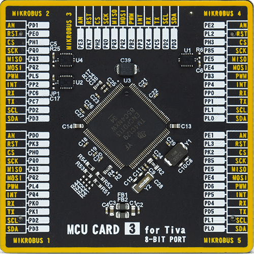
Type
8th Generation
Architecture
ARM Cortex-M4
MCU Memory (KB)
1024
Silicon Vendor
Texas Instruments
Pin count
128
RAM (Bytes)
262144
Used MCU Pins
mikroBUS™ mapper
Take a closer look
Click board™ Schematic

Step by step
Project assembly

Start by selecting your development board and Click board™. Begin with the Fusion for Tiva v8 as your development board.


Software Support
Library Description
This library contains API for Flash 11 Click driver.
Key functions:
flash11_memory_write- Flash 11 memory write function.flash11_memory_read- Flash 11 memory read function.flash11_block_erase- Flash 11 block erase function.
Open Source
Code example
The complete application code and a ready-to-use project are available through the NECTO Studio Package Manager for direct installation in the NECTO Studio. The application code can also be found on the MIKROE GitHub account.
/*!
 * @file main.c
 * @brief Flash 11 Click example
 *
 * # Description
 * This example demonstrates the use of Flash 11 Click board.
 * The demo app writes specified data to the memory and reads it back.
 *
 * The demo application is composed of two sections :
 *
 * ## Application Init
 * The initialization of SPI module, log UART, and additional pins.
 * After the driver init, the app executes a default configuration.
 *
 * ## Application Task
 * This example demonstrates the use of the Flash 11 Click board™.
 * The demo application writes a desired number of bytes to the memory
 * and then verifies if it is written correctly
 * by reading from the same memory location and displaying the memory content.
 * Results are being sent to the UART Terminal, where you can track their changes.
 *
 * @author Nenad Filipovic
 *
 */

#include "board.h"
#include "log.h"
#include "flash11.h"

static flash11_t flash11;
static log_t logger;

#define DEMO_TEXT_MESSAGE_1         "MikroE"
#define STARTING_ADDRESS_1           0x010203ul
#define DEMO_TEXT_MESSAGE_2         "Flash 11 Click"
#define STARTING_ADDRESS_2           0x123456ul

void application_init ( void )
{
    log_cfg_t log_cfg;  /**< Logger config object. */
    flash11_cfg_t flash11_cfg;  /**< Click config object. */

    /**
     * Logger initialization.
     * Default baud rate: 115200
     * Default log level: LOG_LEVEL_DEBUG
     * @note If USB_UART_RX and USB_UART_TX
     * are defined as HAL_PIN_NC, you will
     * need to define them manually for log to work.
     * See @b LOG_MAP_USB_UART macro definition for detailed explanation.
     */
    LOG_MAP_USB_UART( log_cfg );
    log_init( &logger, &log_cfg );
    log_info( &logger, " Application Init " );

    // Click initialization.
    flash11_cfg_setup( &flash11_cfg );
    FLASH11_MAP_MIKROBUS( flash11_cfg, MIKROBUS_1 );
    if ( SPI_MASTER_ERROR == flash11_init( &flash11, &flash11_cfg ) )
    {
        log_error( &logger, " Communication init." );
        for ( ; ; );
    }

    if ( FLASH11_ERROR == flash11_default_cfg ( &flash11 ) )
    {
        log_error( &logger, " Default configuration." );
        for ( ; ; );
    }

    log_info( &logger, " Application Task " );
    log_printf( &logger, " ----------------------------\r\n" );
    Delay_ms ( 100 );
}

void application_task ( void )
{
    uint8_t data_buf[ 128 ] = { 0 };
    log_printf( &logger, " Memory address: 0x%.6LX\r\n", ( uint32_t ) STARTING_ADDRESS_1 );
    if ( FLASH11_OK == flash11_block_erase( &flash11, FLASH11_CMD_BLOCK_ERASE_4KB, STARTING_ADDRESS_1 ) )
    {
        log_printf( &logger, " Erase memory block (4KB)\r\n" );
    }

    memcpy( data_buf, DEMO_TEXT_MESSAGE_1, strlen( DEMO_TEXT_MESSAGE_1 ) );
    if ( FLASH11_OK == flash11_memory_write( &flash11, STARTING_ADDRESS_1, data_buf, sizeof( data_buf ) ) )
    {
        log_printf( &logger, " Write data: %s\r\n", data_buf );
        Delay_ms ( 100 );
    }

    memset( data_buf, 0, sizeof( data_buf ) );
    if ( FLASH11_OK == flash11_memory_read( &flash11, STARTING_ADDRESS_1, data_buf, sizeof( data_buf ) ) )
    {
        log_printf( &logger, " Read data: %s\r\n", data_buf );
        Delay_ms ( 1000 );
        Delay_ms ( 1000 );
        Delay_ms ( 1000 );
    }
    log_printf( &logger, " ----------------------------\r\n" );

    log_printf( &logger, " Memory address: 0x%.6LX\r\n", ( uint32_t ) STARTING_ADDRESS_2 );
    if ( FLASH11_OK == flash11_block_erase( &flash11, FLASH11_CMD_BLOCK_ERASE_4KB, STARTING_ADDRESS_2 ) )
    {
        log_printf( &logger, " Erase memory block (4KB)\r\n" );
    }

    memcpy( data_buf, DEMO_TEXT_MESSAGE_2, strlen( DEMO_TEXT_MESSAGE_2 ) );
    if ( FLASH11_OK == flash11_memory_write( &flash11, STARTING_ADDRESS_2, data_buf, sizeof( data_buf ) ) )
    {
        log_printf( &logger, " Write data: %s\r\n", data_buf );
        Delay_ms ( 100 );
    }

    memset( data_buf, 0, sizeof( data_buf ) );
    if ( FLASH11_OK == flash11_memory_read( &flash11, STARTING_ADDRESS_2, data_buf, sizeof( data_buf ) ) )
    {
        log_printf( &logger, " Read data: %s\r\n", data_buf );
        Delay_ms ( 1000 );
        Delay_ms ( 1000 );
        Delay_ms ( 1000 );
    }
    log_printf ( &logger, " ----------------------------\r\n" );
}

int main ( void )
{
    /* Do not remove this line or clock might not be set correctly. */
    #ifdef PREINIT_SUPPORTED
    preinit();
    #endif

    application_init( );

    for ( ; ; )
    {
        application_task( );
    }

    return 0;
}

// ------------------------------------------------------------------------ END


