Bridge the gap between the digital and analog world with DAC80501 and STM32F302VC
Craft your analog path with DAC innovation
Published Jul 22, 2025
Click board™
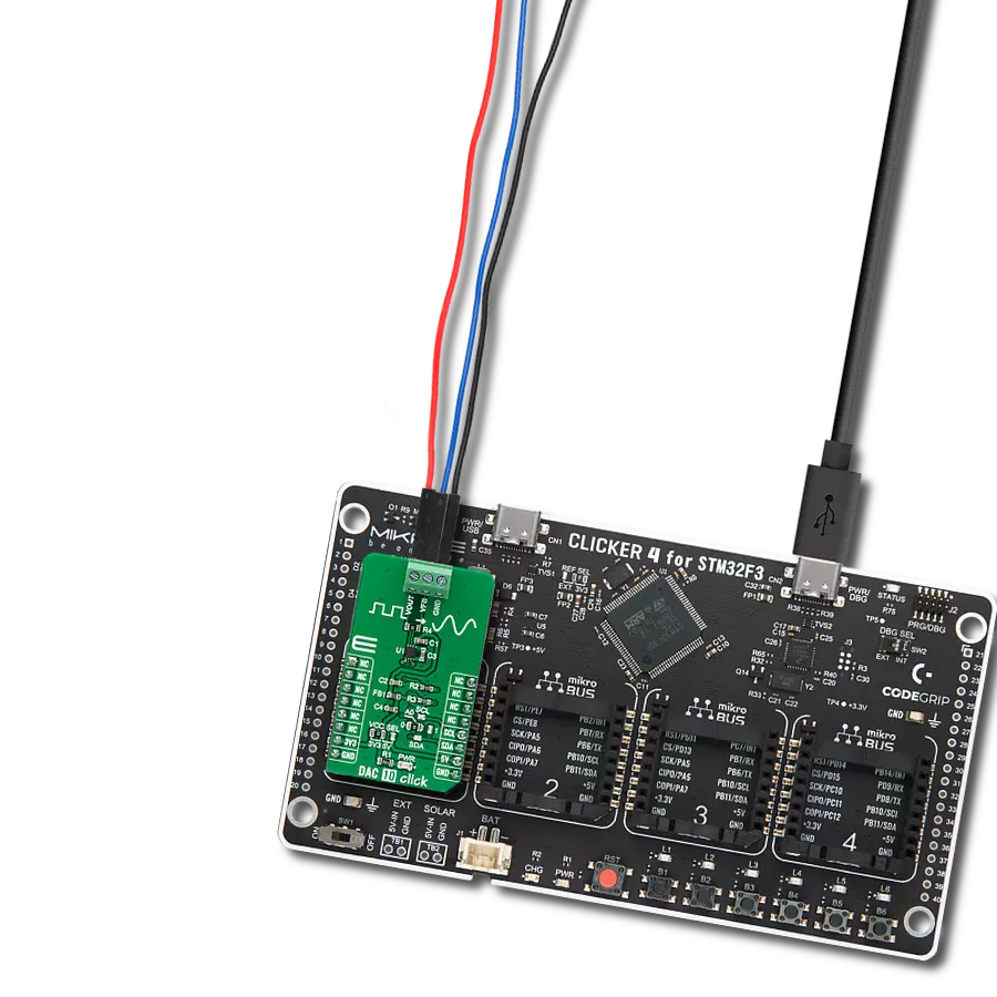
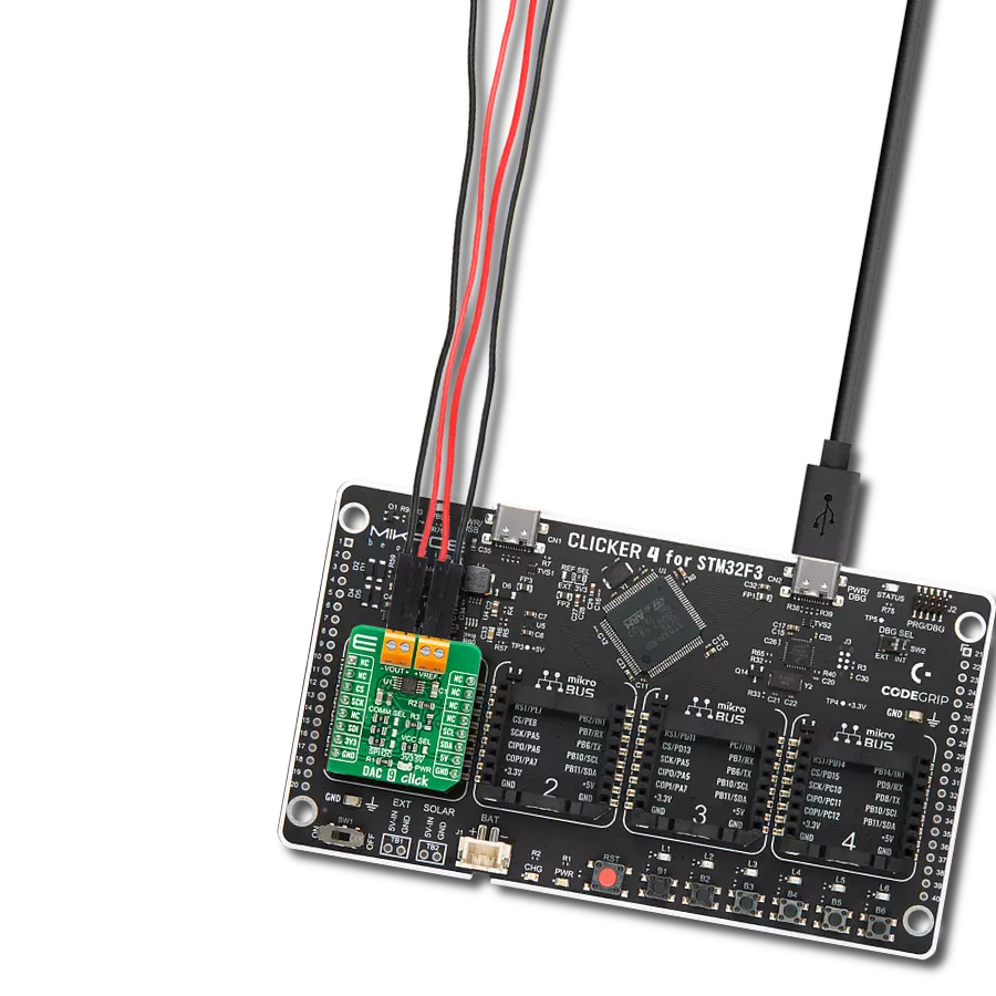
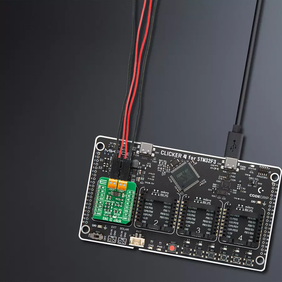
DAC 9 Click
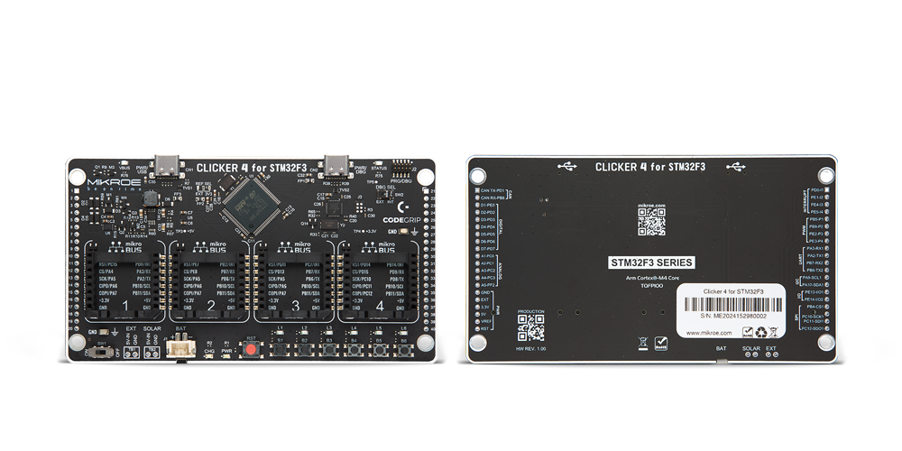
Dev. board
CLICKER 4 for STM32F302VCT6
Compiler
NECTO Studio
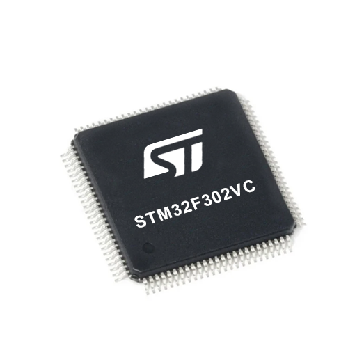
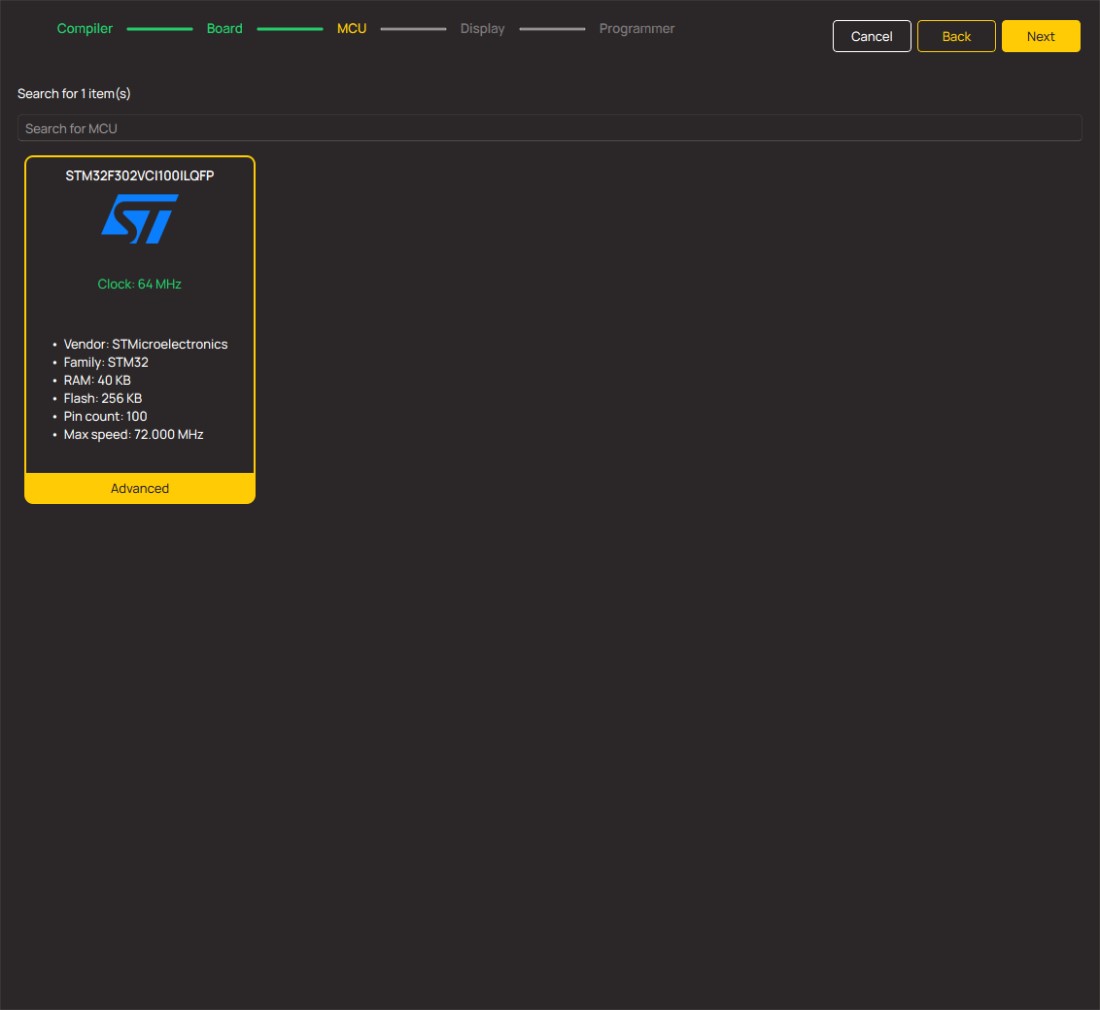
MCU
STM32F302VC
By translating binary codes into voltage levels, this solution amplifies data's voice, enabling systems to interpret, respond to, and leverage digital insights for various applications
A
A
Hardware Overview
How does it work?
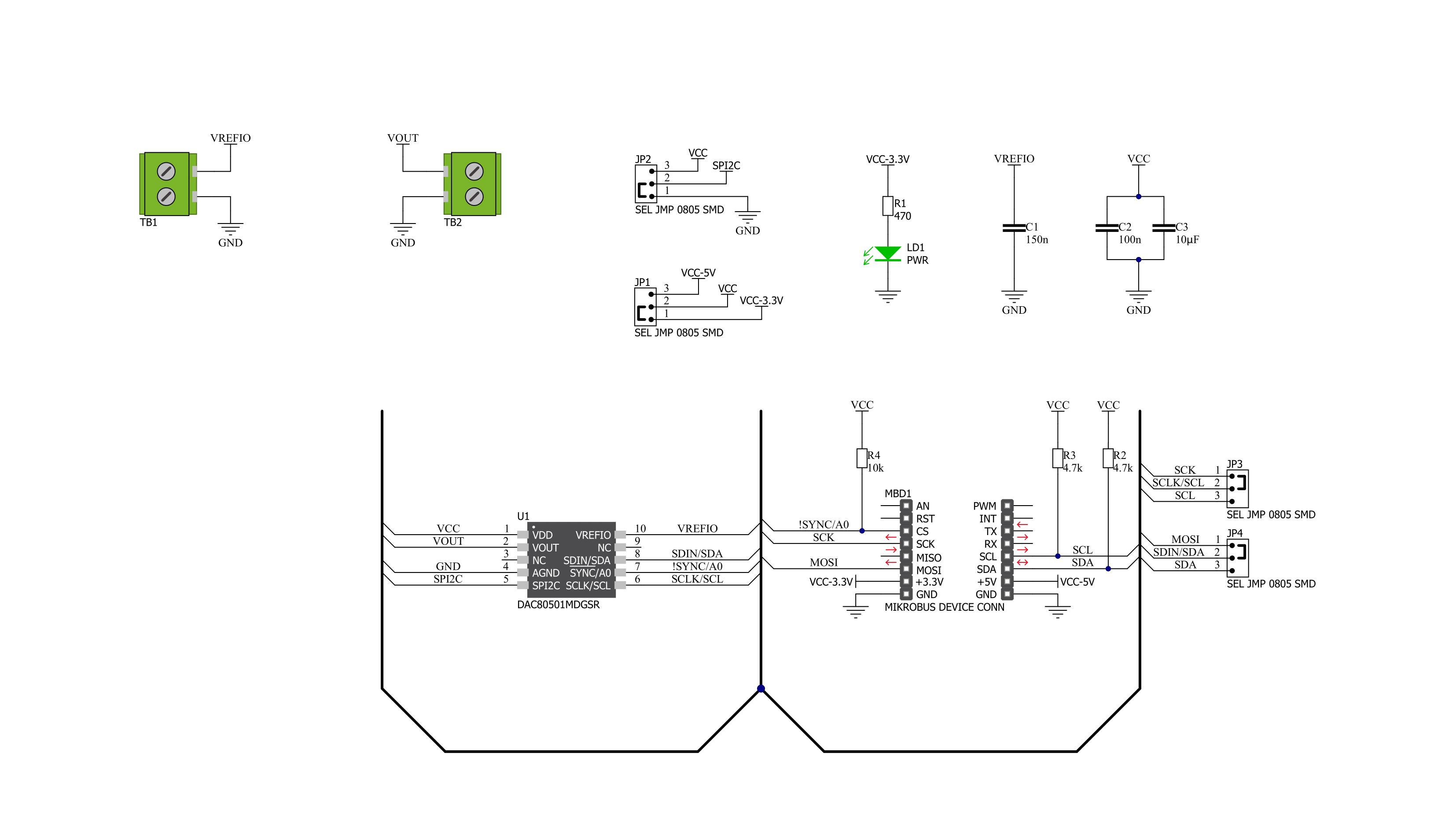
DAC 9 Click is based on the DAC80501, a single-channel, buffered, 16-bit resolution digital-to-analog converter from Texas Instruments. It includes a 2.5V, 5ppm/˚C internal reference, giving full-scale output voltage ranges of 1.25V, 2.5V, or 5V, and incorporates a Power-On Reset function. This function makes sure that the DAC80501 output powers up at zero scale or midscale and remains at that scale until a valid code is written to the device. High resolution and simple interface features make this Click board™ suitable for applications such as battery testers, communications equipment, factory automation, control, test and measurement, and more. The output channel, which DAC80501 routed to the VOUT terminal, consists of a rail-to-rail ladder
architecture with an output buffer amplifier that generates rail-to-rail voltages, giving a maximum output range of 0V to VDD. The full-scale output range of the DAC output is determined by the reference voltage on the VREFIO pin, the reference divider setting, and the gain configuration for that channel set by the corresponding BUFF-GAIN bit. When the DAC80501 uses an internal reference, this voltage is externally available at the VREF terminal and can source up to 5mA. Besides, the user can bring the external reference voltage on this terminal in the case of the DAC80501 external reference configuration. DAC 9 Click provides the possibility of using both I2C and SPI interfaces. The selection can be performed by positioning SMD jumpers labeled COMM SEL to an appropriate
position. Note that all jumpers must be placed on the same side, or the Click board™ may become unresponsive. In SPI mode, the DAC80501 uses a 3-Wire SPI serial interface that operates at clock rates of up to 50MHz, while in I2C mode, the DAC80501 can operate in Standard Mode (100 kbps), Fast Mode (400 kbps) and Fast-Plus Mode (1.0 Mbps). This Click board™ can operate with either 3.3V or 5V logic voltage levels selected via the VCC SEL jumper. This way, both 3.3V and 5V capable MCUs can use the communication lines properly. Also, this Click board™ comes equipped with a library containing easy-to-use functions and an example code that can be used, as a reference, for further development.

Features overview
Development board
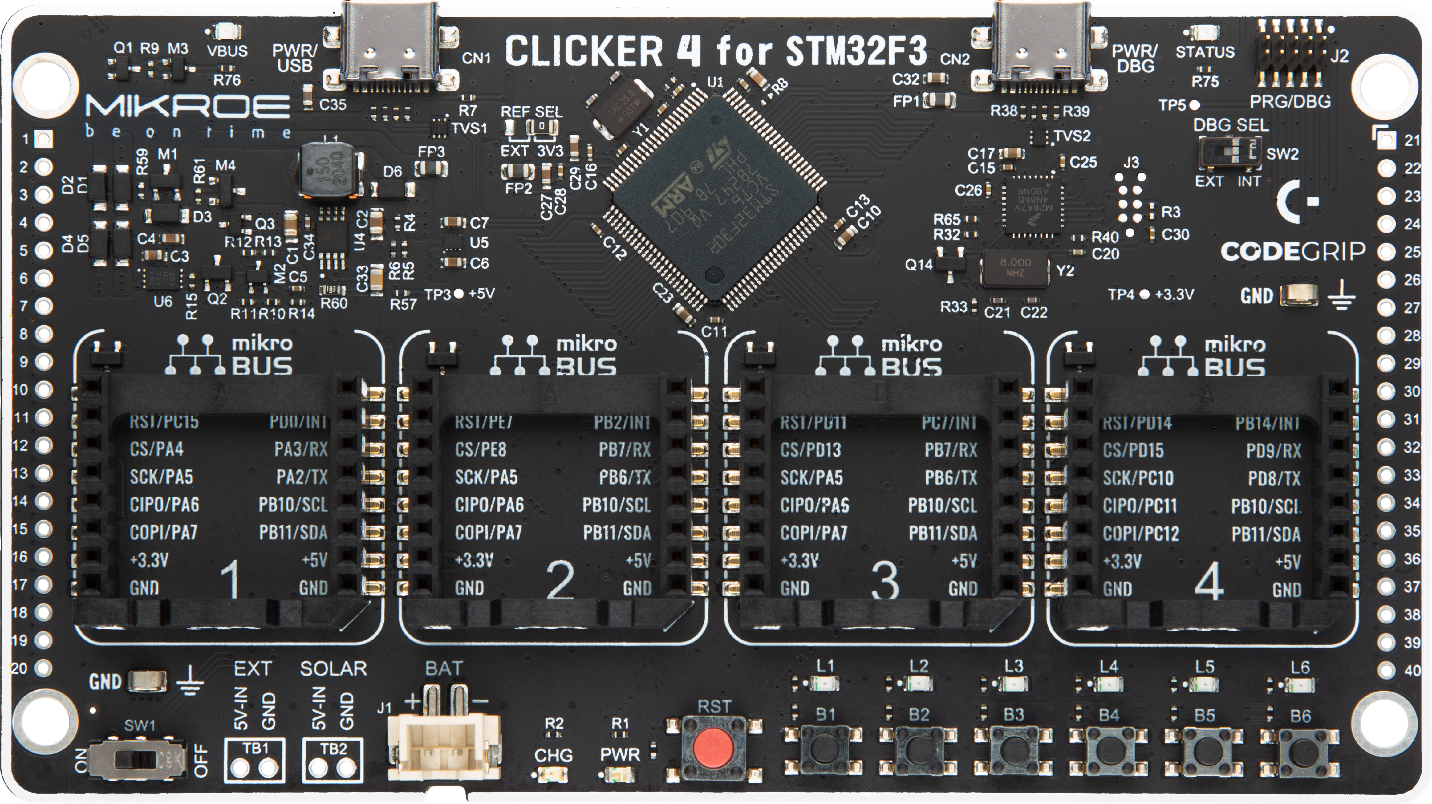
Clicker 4 for STM32F3 is a compact development board designed as a complete solution, you can use it to quickly build your own gadgets with unique functionalities. Featuring a STM32F302VCT6, four mikroBUS™ sockets for Click boards™ connectivity, power managment, and more, it represents a perfect solution for the rapid development of many different types of applications. At its core, there is a STM32F302VCT6 MCU, a powerful microcontroller by STMicroelectronics, based on the high-
performance Arm® Cortex®-M4 32-bit processor core operating at up to 168 MHz frequency. It provides sufficient processing power for the most demanding tasks, allowing Clicker 4 to adapt to any specific application requirements. Besides two 1x20 pin headers, four improved mikroBUS™ sockets represent the most distinctive connectivity feature, allowing access to a huge base of Click boards™, growing on a daily basis. Each section of Clicker 4 is clearly marked, offering an intuitive and clean interface. This makes working with the development
board much simpler and thus, faster. The usability of Clicker 4 doesn’t end with its ability to accelerate the prototyping and application development stages: it is designed as a complete solution which can be implemented directly into any project, with no additional hardware modifications required. Four mounting holes [4.2mm/0.165”] at all four corners allow simple installation by using mounting screws. For most applications, a nice stylish casing is all that is needed to turn the Clicker 4 development board into a fully functional, custom design.
Microcontroller Overview
MCU Card / MCU
Architecture
ARM Cortex-M4
MCU Memory (KB)
256
Silicon Vendor
STMicroelectronics
Pin count
100
RAM (Bytes)
40960
Used MCU Pins
mikroBUS™ mapper
Take a closer look
Click board™ Schematic
Step by step
Project assembly
Start by selecting your development board and Click board™. Begin with the CLICKER 4 for STM32F302VCT6 as your development board.


Track your results in real time
Application Output
1. Application Output - In Debug mode, the 'Application Output' window enables real-time data monitoring, offering direct insight into execution results. Ensure proper data display by configuring the environment correctly using the provided tutorial.

2. UART Terminal - Use the UART Terminal to monitor data transmission via a USB to UART converter, allowing direct communication between the Click board™ and your development system. Configure the baud rate and other serial settings according to your project's requirements to ensure proper functionality. For step-by-step setup instructions, refer to the provided tutorial.

3. Plot Output - The Plot feature offers a powerful way to visualize real-time sensor data, enabling trend analysis, debugging, and comparison of multiple data points. To set it up correctly, follow the provided tutorial, which includes a step-by-step example of using the Plot feature to display Click board™ readings. To use the Plot feature in your code, use the function: plot(*insert_graph_name*, variable_name);. This is a general format, and it is up to the user to replace 'insert_graph_name' with the actual graph name and 'variable_name' with the parameter to be displayed.

Software Support
Library Description
This library contains API for DAC 9 Click driver.
Key functions:
dac9_set_config- Set config functiondac9_set_gain- Set gain functiondac9_set_vout- Set Vout function
Open Source
Code example
The complete application code and a ready-to-use project are available through the NECTO Studio Package Manager for direct installation in the NECTO Studio. The application code can also be found on the MIKROE GitHub account.
/*!
 * @file main.c
 * @brief DAC9 Click example
 *
 * # Description
 * This is an example that demonstrates the use of the DAC 9 Click board.
 *
 * The demo application is composed of two sections :
 *
 * ## Application Init
 * Initalizes SPI or I2C driver and applies default settings.
 *
 * ## Application Task
 * Demonstrates use of DAC 9 Click board by changing output values every two seconds.
 *
 * @author Stefan Ilic
 *
 */

#include "board.h"
#include "log.h"
#include "dac9.h"

static dac9_t dac9;
static log_t logger;
static uint16_t res = 2500;

void application_init ( void ) {
    log_cfg_t log_cfg;  /**< Logger config object. */
    dac9_cfg_t dac9_cfg;  /**< Click config object. */

    /**
     * Logger initialization.
     * Default baud rate: 115200
     * Default log level: LOG_LEVEL_DEBUG
     * @note If USB_UART_RX and USB_UART_TX
     * are defined as HAL_PIN_NC, you will
     * need to define them manually for log to work.
     * See @b LOG_MAP_USB_UART macro definition for detailed explanation.
     */
    LOG_MAP_USB_UART( log_cfg );
    log_init( &logger, &log_cfg );
    log_info( &logger, " Application Init " );

    // Click initialization.
    dac9_cfg_setup( &dac9_cfg );
    DAC9_MAP_MIKROBUS( dac9_cfg, MIKROBUS_1 );
    err_t init_flag  = dac9_init( &dac9, &dac9_cfg );
    if ( ( I2C_MASTER_ERROR == init_flag ) || ( SPI_MASTER_ERROR == init_flag ) ) {
        log_error( &logger, " Application Init Error. " );
        log_info( &logger, " Please, run program again... " );

        for ( ; ; );
    }
    log_printf( &logger, "---------------------\r\n" );
    log_printf( &logger, "     Soft reset      \r\n" );
    dac9_soft_reset( &dac9 );
    Delay_ms ( 200 );

    log_printf( &logger, "---------------------\r\n" );
    log_printf( &logger, "  Vref divided by 2  \r\n" );
    log_printf( &logger, "  Set DAC gain of 2  \r\n" );
    dac9_set_gain( &dac9, DAC9_GAIN_REF_DIV_2, DAC9_GAIN_BUFF_GAIN_2 );
    Delay_ms ( 100 );

    log_printf( &logger, "---------------------\r\n" );
    log_info( &logger, " Application Task " );
}

void application_task ( void ) {
    uint16_t n_cnt;
    for ( n_cnt = 0; n_cnt <= res; n_cnt += 500 ) {
        log_printf( &logger, "Output Voltage : %d mV\r\n", ( uint16_t ) n_cnt );
        dac9_set_vout( &dac9, n_cnt );
        Delay_ms ( 1000 );
        Delay_ms ( 1000 );
    }
}

int main ( void )
{
    /* Do not remove this line or clock might not be set correctly. */
    #ifdef PREINIT_SUPPORTED
    preinit();
    #endif

    application_init( );

    for ( ; ; )
    {
        application_task( );
    }

    return 0;
}

// ------------------------------------------------------------------------ END
Additional Support
Resources
Category:DAC