Develop data storage and transfer solution with EN25Q80B and TM4C129ENCPDT
Highly reliable serial flash memory with a capacity of 8Mbits
Published Aug 25, 2023
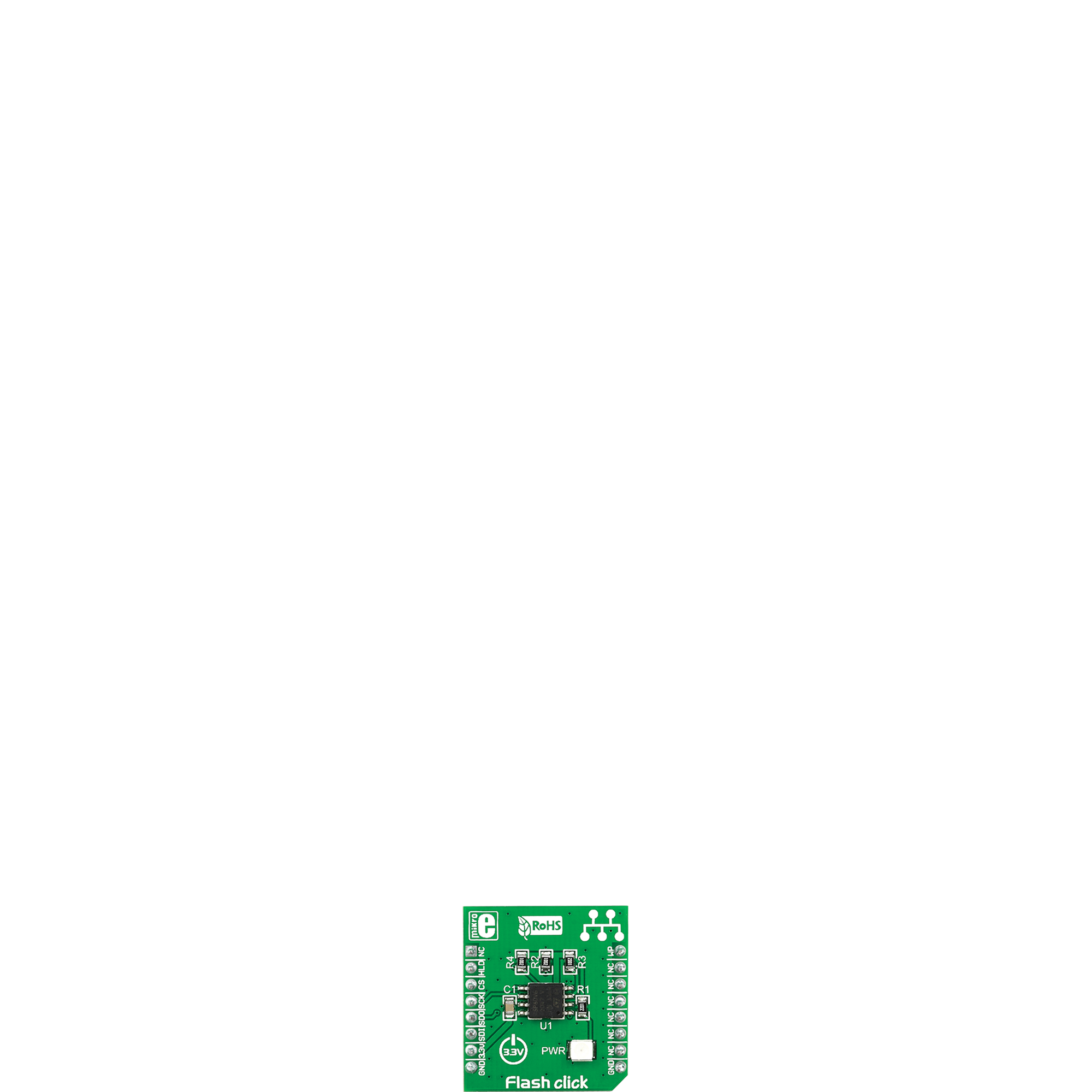
Click board™
Flash Click
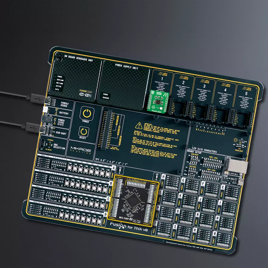
Dev. board
Fusion for Tiva v8
Compiler
NECTO Studio
MCU
TM4C129ENCPDT
Robust and reliable memory solution with a decent storage capacity, advanced write protection, and excellent endurance
A
A
Hardware Overview
How does it work?
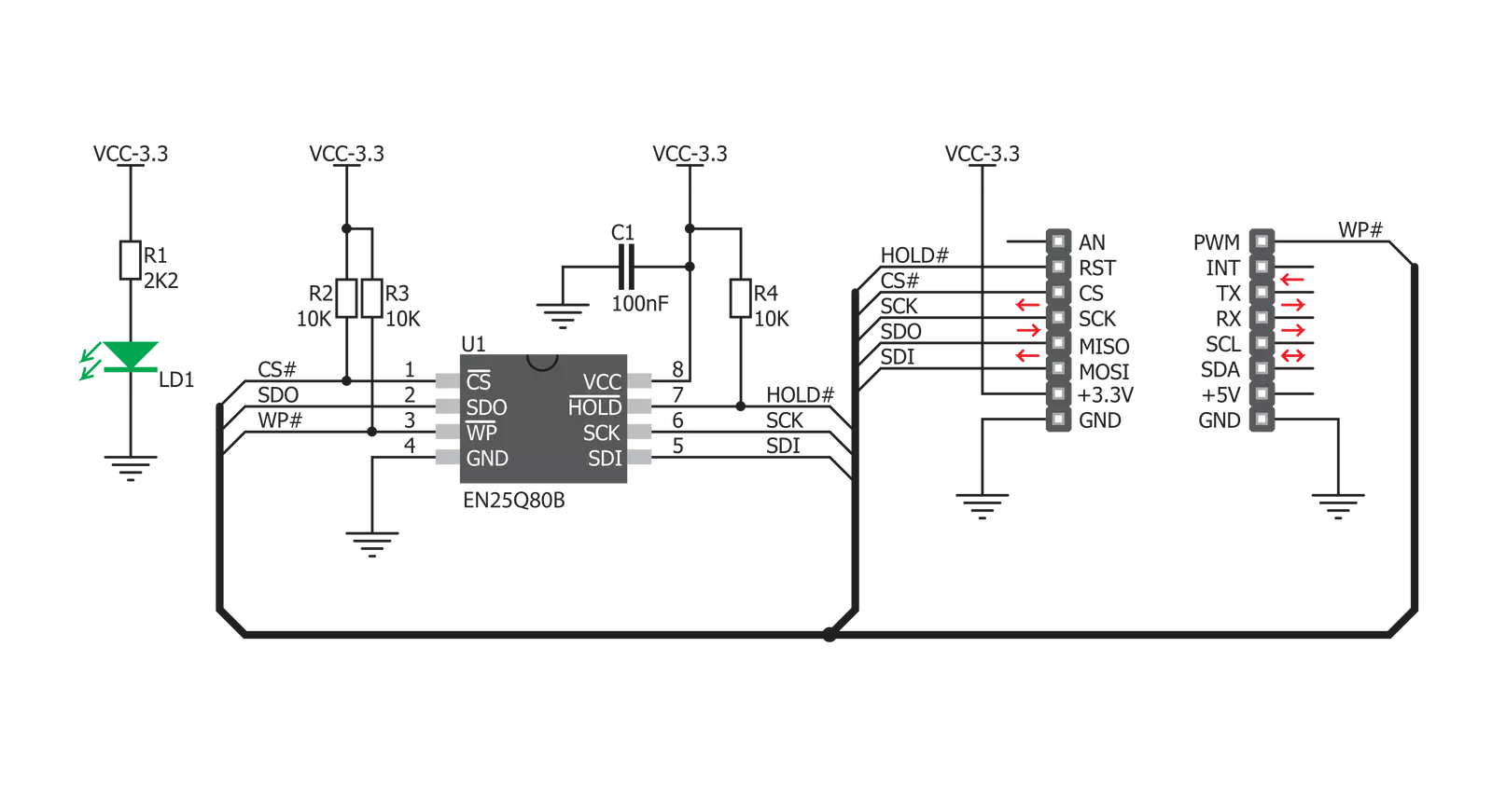
Flash Click is based on the EN25Q80B, a serial flash memory from EON Silicon Solutions. The EN25Q80B features Serial Flash Discoverable Parameters (SFDP) mode, used to retrieve advanced information from the device, such as the operating characteristics, structure and vendor-specified information, memory size, operating voltage, timing information, and more. Page Program instruction allows up to 256 bytes to be written during one write cycle, although it is possible to write less than that. By automatically incrementing the addresses, it is possible to read the entire memory by a single command. The
EN25Q80B allows the erasure of one sector at a time, half a block at a time, block at a time, and the entire memory. The addition of 512 bytes of one-time programmable (OTP) memory can be useful for building secure storage devices and similar secure storage applications. Flash Click uses a standard 4-Wire SPI serial interface to communicate with the host MCU, supporting Dual SPI and Quad SPI modes, which utilize these two additional modes, allowing faster data transfer speeds several times. There are additional WP for the write protect function and HLD pins. If using Quad SPI, the SDI and SDO become DQ0 and
DQ1, while WP and HLD become DQ2 and DQ3, respectively. Due to a small number of MCUs that support Dual and Quad SPI, MIKROE offers library functions that work only with standard SPI communication, ensuring absolute compatibility with all the supported MCUs. This Click board™ can be operated only with a 3.3V logic voltage level. The board must perform appropriate logic voltage level conversion before using MCUs with different logic levels. Also, it comes equipped with a library containing functions and an example code that can be used as a reference for further development.

Features overview
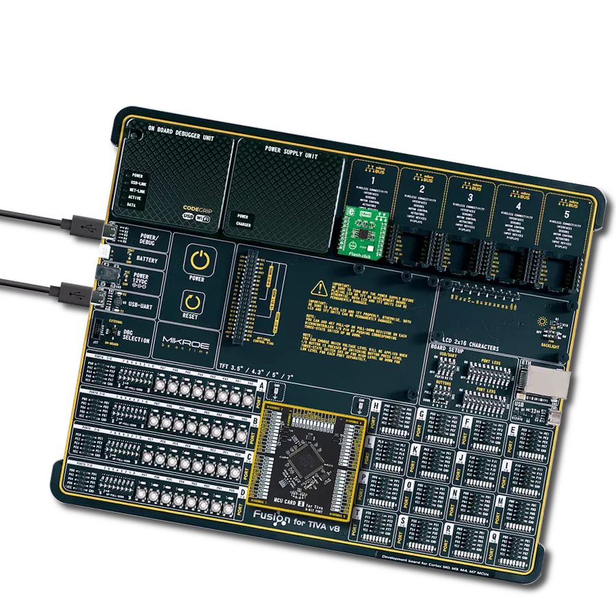
Development board
Fusion for TIVA v8 is a development board specially designed for the needs of rapid development of embedded applications. It supports a wide range of microcontrollers, such as different 32-bit ARM® Cortex®-M based MCUs from Texas Instruments, regardless of their number of pins, and a broad set of unique functions, such as the first-ever embedded debugger/programmer over a WiFi network. The development board is well organized and designed so that the end-user has all the necessary elements, such as switches, buttons, indicators, connectors, and others, in one place. Thanks to innovative manufacturing technology, Fusion for TIVA v8 provides a fluid and immersive working experience, allowing access
anywhere and under any circumstances at any time. Each part of the Fusion for TIVA v8 development board contains the components necessary for the most efficient operation of the same board. An advanced integrated CODEGRIP programmer/debugger module offers many valuable programming/debugging options, including support for JTAG, SWD, and SWO Trace (Single Wire Output)), and seamless integration with the Mikroe software environment. Besides, it also includes a clean and regulated power supply module for the development board. It can use a wide range of external power sources, including a battery, an external 12V power supply, and a power source via the USB Type-C (USB-C) connector.
Communication options such as USB-UART, USB HOST/DEVICE, CAN (on the MCU card, if supported), and Ethernet is also included. In addition, it also has the well-established mikroBUS™ standard, a standardized socket for the MCU card (SiBRAIN standard), and two display options for the TFT board line of products and character-based LCD. Fusion for TIVA v8 is an integral part of the Mikroe ecosystem for rapid development. Natively supported by Mikroe software tools, it covers many aspects of prototyping and development thanks to a considerable number of different Click boards™ (over a thousand boards), the number of which is growing every day.

Microcontroller Overview
MCU Card / MCU
Type
8th Generation
Architecture
ARM Cortex-M4
MCU Memory (KB)
1024
Silicon Vendor
Texas Instruments
Pin count
128
RAM (Bytes)
262144
Used MCU Pins
mikroBUS™ mapper
Take a closer look
Click board™ Schematic
Step by step
Project assembly

Start by selecting your development board and Click board™. Begin with the Fusion for Tiva v8 as your development board.


Software Support
Library Description
This library contains API for Flash Click driver.
Key functions:
flash_write_page- Page Write functionflash_read_page- Page Read functionflash_erase_sector- Sector Erase function
Open Source
Code example
The complete application code and a ready-to-use project are available through the NECTO Studio Package Manager for direct installation in the NECTO Studio. The application code can also be found on the MIKROE GitHub account.
/*!
 * \file main.c
 * \brief Flash Click example
 *
 * # Description
 * This example demonstrates the use (control) of the FLASH memory.
 *
 * The demo application is composed of two sections :
 *
 * ## Application Init
 * Initializes all necessary peripherals and pins used by Flash Click and also
 * initializes uart logger to show results.
 *
 * ## Application Task
 * Executes memory data writing, reading from the memory to verify data writing
 * operation and sector erasing to clear memory.
 *
 * ## Additional Functions
 * - Enter Data / Allows user to enter a desired data.
 * - Process Wait / Makes a delay to wait while some process be done.
 *
 * \author Nemanja Medakovic
 *
 */
// ------------------------------------------------------------------- INCLUDES

#include <string.h>
#include "board.h"
#include "log.h"
#include "flash.h"

// ------------------------------------------------------------------ VARIABLES

static flash_t flash;
static log_t logger;
static uint8_t data_buf[ 30 ];
static uint8_t n_data;

// ------------------------------------------------------- ADDITIONAL FUNCTIONS

void enter_data( unsigned char *buffer )
{
    uint8_t data_size;

    data_size = sizeof( data_buf );

    memset( data_buf, 0, data_size );
    n_data = 0;
    data_size--;

    while ( ( *buffer != 0 ) && ( data_size > 0 ) )
    {
        data_buf[ n_data ] = *buffer;
        buffer++;
        n_data++;
        data_size--;
    }
}

void process_wait( void )
{
    uint8_t cnt;

    for ( cnt = 0; cnt < 9; cnt++ )
    {
        Delay_ms ( 400 );
        log_printf( &logger, "****" );
    }

    log_printf( &logger, "\r\n" );
    Delay_ms ( 400 );
}

// ------------------------------------------------------ APPLICATION FUNCTIONS

void application_init( void )
{
    flash_cfg_t flash_cfg;
    log_cfg_t log_cfg;

    /**
     * Logger initialization.
     * Default baud rate: 115200
     * Default log level: LOG_LEVEL_DEBUG
     * @note If USB_UART_RX and USB_UART_TX
     * are defined as HAL_PIN_NC, you will
     * need to define them manually for log to work.
     * See @b LOG_MAP_USB_UART macro definition for detailed explanation.
     */
    LOG_MAP_USB_UART( log_cfg );
    log_init( &logger, &log_cfg );
    log_info( &logger, "---- Application Init ----" );

    //  Click initialization.
    flash_cfg_setup( &flash_cfg );
    FLASH_MAP_MIKROBUS( flash_cfg, MIKROBUS_1 );
    flash_init( &flash, &flash_cfg );

    //  Click reset and default configuration.
    flash_reset( &flash );
    flash_default_cfg( &flash );

    log_printf( &logger, "***  Flash Initialization Done.  ***\r\n" );
    log_printf( &logger, "************************************\r\n" );
}

void application_task( void )
{
    enter_data( "Mikroelektronika (MikroE)" );

    log_printf( &logger, "> Data content to be written: %s\r\n", data_buf );
    log_printf( &logger, "> Data writing to memory...\r\n" );
    flash_write_page( &flash, FLASH_MEM_ADDR_FIRST_PAGE_START, data_buf, n_data );
    log_printf( &logger, "> Done.\r\n" );

    memset( data_buf, 0, sizeof( data_buf ) );
    process_wait( );

    log_printf( &logger, "> Data reading from memory...\r\n" );
    flash_read_page( &flash, FLASH_MEM_ADDR_FIRST_PAGE_START, data_buf, n_data );
    log_printf( &logger, "> Done.\r\n> Read data content: %s\r\n", data_buf );

    process_wait( );

    log_printf( &logger, "> Sector erasing...\r\n" );
    flash_erase_sector( &flash, FLASH_MEM_ADDR_FIRST_SECTOR_START );
    log_printf( &logger, "> Done.\r\n" );

    process_wait( );
}

int main ( void )
{
    /* Do not remove this line or clock might not be set correctly. */
    #ifdef PREINIT_SUPPORTED
    preinit();
    #endif

    application_init( );

    for ( ; ; )
    {
        application_task( );
    }

    return 0;
}


// ------------------------------------------------------------------------ END


