Achieve safety isolation from high voltage with ISOM8710 and PIC18F86J50
High voltage, low worries

Published Dec 19, 2023
Click board™
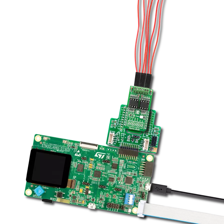
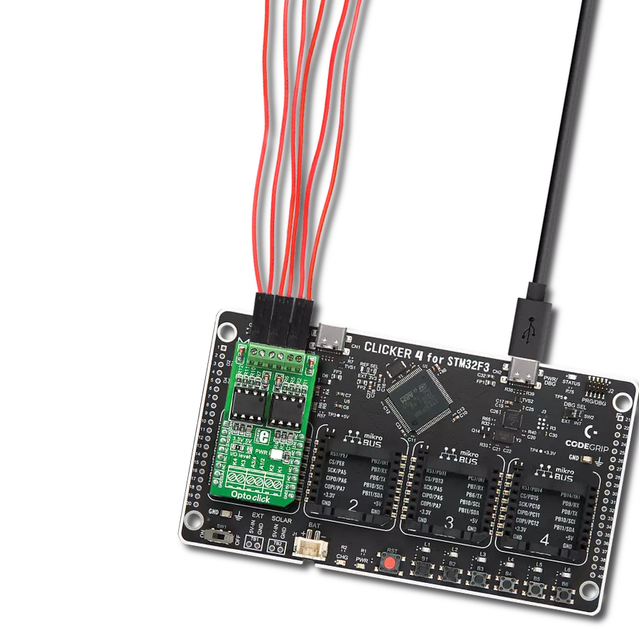
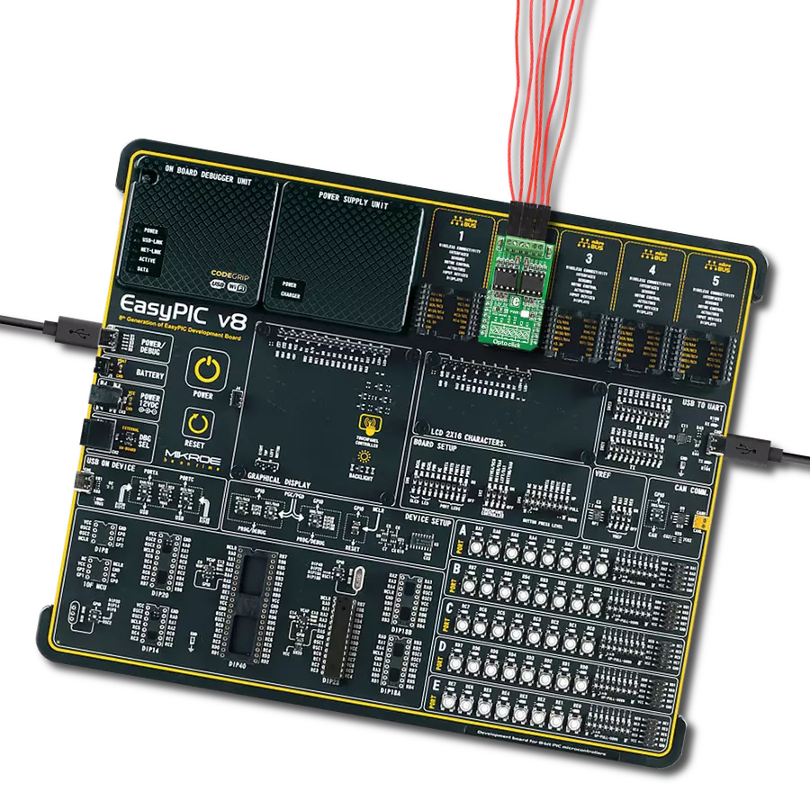
Opto 7 Click
Dev. board
UNI-DS v8
Compiler
NECTO Studio
MCU
PIC18F86J50
Safety shield that you can add to electronic systems, especially in applications like power supplies, electricity meters, motor drives, and automation systems
A
A
Hardware Overview
How does it work?
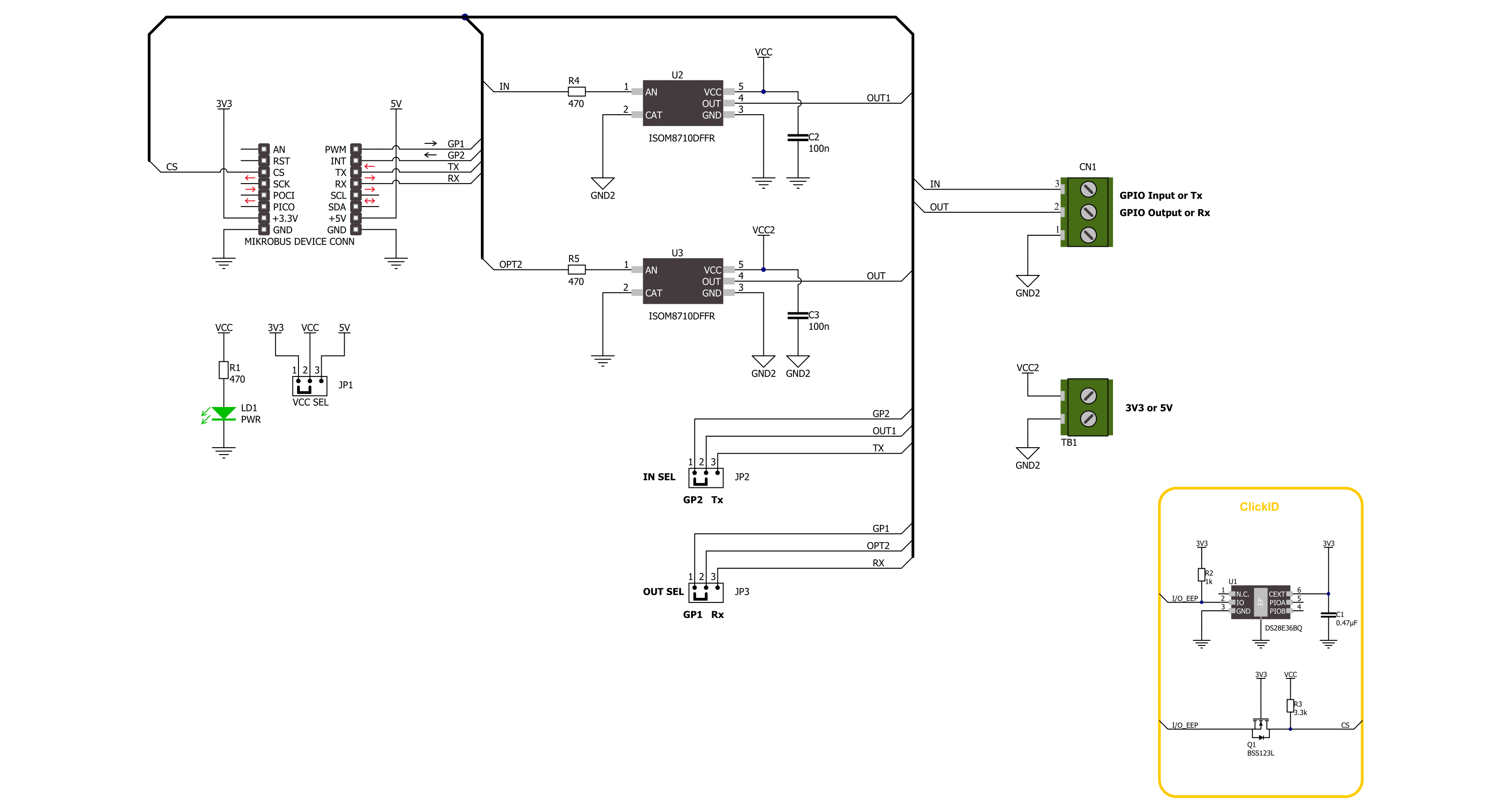
Opto 7 Click is based on two ISOM8710s, high-speed single-channel opto-emulators from Texas Instruments. It can transmit data rates of up to 25Mbps and output 3.3V and 5V signals with a CMOS-compatible output. Compared to an optocoupler, the ISOM7810 has a high common mode transient immunity, low propagation delay, small pulse with distortion, low power consumption, and more. Opto 7 Click is equipped with two of these opto-emulators for receiving and transmitting
data. The external power supply can be connected to a VCC2 terminal and must be 3.3V or 5V. The three-pin terminal connects input and output data lines along with the common ground. Opto 7 Click can use general-purpose IO to communicate with the host MCU over the GP1 and GP2 pins. It can also be used for a standard UART communication isolation with commonly used UART RX and TX pins. The selection can be made over the OUT SEL and IN SEL jumpers. Both should be in a proper
position for the communication to work. This Click board™ can operate with either 3.3V or 5V logic voltage levels selected via the VCC SEL jumper. This way, both 3.3V and 5V capable MCUs can use the communication lines properly. Also, this Click board™ comes equipped with a library containing easy-to-use functions and an example code that can be used as a reference for further development.

Features overview
Development board
UNI-DS v8 is a development board specially designed for the needs of rapid development of embedded applications. It supports a wide range of microcontrollers, such as different STM32, Kinetis, TIVA, CEC, MSP, PIC, dsPIC, PIC32, and AVR MCUs regardless of their number of pins, and a broad set of unique functions, such as the first-ever embedded debugger/programmer over WiFi. The development board is well organized and designed so that the end-user has all the necessary elements, such as switches, buttons, indicators, connectors, and others, in one place. Thanks to innovative manufacturing technology, UNI-DS v8 provides a fluid and immersive working experience, allowing access anywhere and under any
circumstances at any time. Each part of the UNI-DS v8 development board contains the components necessary for the most efficient operation of the same board. An advanced integrated CODEGRIP programmer/debugger module offers many valuable programming/debugging options, including support for JTAG, SWD, and SWO Trace (Single Wire Output)), and seamless integration with the Mikroe software environment. Besides, it also includes a clean and regulated power supply module for the development board. It can use a wide range of external power sources, including a battery, an external 12V power supply, and a power source via the USB Type-C (USB-C) connector. Communication options such as USB-UART, USB
HOST/DEVICE, CAN (on the MCU card, if supported), and Ethernet is also included. In addition, it also has the well-established mikroBUS™ standard, a standardized socket for the MCU card (SiBRAIN standard), and two display options for the TFT board line of products and character-based LCD. UNI-DS v8 is an integral part of the Mikroe ecosystem for rapid development. Natively supported by Mikroe software tools, it covers many aspects of prototyping and development thanks to a considerable number of different Click boards™ (over a thousand boards), the number of which is growing every day.

Microcontroller Overview
MCU Card / MCU
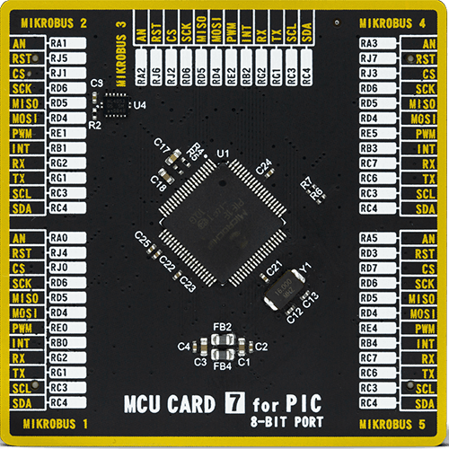
Type
8th Generation
Architecture
PIC
MCU Memory (KB)
64
Silicon Vendor
Microchip
Pin count
80
RAM (Bytes)
3904
Used MCU Pins
mikroBUS™ mapper
Take a closer look
Click board™ Schematic
Step by step
Project assembly

Start by selecting your development board and Click board™. Begin with the UNI-DS v8 as your development board.


Track your results in real time
Application Output
1. Application Output - In Debug mode, the 'Application Output' window enables real-time data monitoring, offering direct insight into execution results. Ensure proper data display by configuring the environment correctly using the provided tutorial.

2. UART Terminal - Use the UART Terminal to monitor data transmission via a USB to UART converter, allowing direct communication between the Click board™ and your development system. Configure the baud rate and other serial settings according to your project's requirements to ensure proper functionality. For step-by-step setup instructions, refer to the provided tutorial.

3. Plot Output - The Plot feature offers a powerful way to visualize real-time sensor data, enabling trend analysis, debugging, and comparison of multiple data points. To set it up correctly, follow the provided tutorial, which includes a step-by-step example of using the Plot feature to display Click board™ readings. To use the Plot feature in your code, use the function: plot(*insert_graph_name*, variable_name);. This is a general format, and it is up to the user to replace 'insert_graph_name' with the actual graph name and 'variable_name' with the parameter to be displayed.

Software Support
Library Description
This library contains API for Opto 7 Click driver.
Key functions:
opto7_generic_write- Opto 7 data writing function.opto7_set_gp1_pin- Opto 7 set GP1 pin function.opto7_get_gp2_pin- Opto 7 get GP2 pin function.
Open Source
Code example
The complete application code and a ready-to-use project are available through the NECTO Studio Package Manager for direct installation in the NECTO Studio. The application code can also be found on the MIKROE GitHub account.
/*!
 * @file main.c
 * @brief Opto 7 Click Example.
 *
 * # Description
 * This example demonstrates the use of Opto 7 Click board by processing
 * the incoming data and displaying them on the USB UART.
 *
 * The demo application is composed of two sections :
 *
 * ## Application Init
 * Initialization of UART LOG and GPIO pin, and UART drivers.
 *
 * ## Application Task
 * This example is made of two parts:
 * GPIO Example - The output pin is toggled every 5 seconds and input pin state is being tracked.
 * UART Example - Device assigned as transmitter is sending message and receiver is reading it and displaying it on USB UART.
 *
 * ## Additional Function
 * - static void opto7_clear_app_buf ( void )
 * - static void opto7_log_app_buf ( void )
 * - static err_t opto7_process ( opto7_t *ctx )
 *
 * @author Stefan Ilic
 *
 */

#include "board.h"
#include "log.h"
#include "opto7.h"

// Example selection macros
#define EXAMPLE_GPIO                1               // Example of using GPIO
#define EXAMPLE_UART                2               // Example of using UART
#define DEMO_EXAMPLE                EXAMPLE_GPIO    // Example selection macro

// Macros for UART example
#define TRANSMITTER                 // Comment out this line to place device into receiver mode
#define TX_MESSAGE                  "Opto 7 Click Example \r\n"

// Application buffer size
#define APP_BUFFER_SIZE             500
#define PROCESS_BUFFER_SIZE         200

static opto7_t opto7;
static log_t logger;


static uint8_t app_buf[ APP_BUFFER_SIZE ] = { 0 };
static int32_t app_buf_len = 0;

/**
 * @brief Test clearing application buffer.
 * @details This function clears memory of application buffer and reset its length.
 * @note None.
 */
static void opto7_clear_app_buf ( void );

/**
 * @brief Test log application buffer.
 * @details This function logs data from application buffer to USB UART.
 * @note None.
 */
static void opto7_log_app_buf ( void );

/**
 * @brief Test data reading function.
 * @details This function reads data from device and concatenates data to application buffer.
 * @param[in] ctx : Click context object.
 * See #opto7_t object definition for detailed explanation.
 * @return @li @c  0 - Read some data.
 *         @li @c -1 - Nothing is read.
 * See #err_t definition for detailed explanation.
 * @note None.
 */
static err_t opto7_process ( opto7_t *ctx );

void application_init ( void )
{
    log_cfg_t log_cfg;  /**< Logger config object. */
    opto7_cfg_t opto7_cfg;  /**< Click config object. */

    /**
     * Logger initialization.
     * Default baud rate: 115200
     * Default log level: LOG_LEVEL_DEBUG
     * @note If USB_UART_RX and USB_UART_TX
     * are defined as HAL_PIN_NC, you will
     * need to define them manually for log to work.
     * See @b LOG_MAP_USB_UART macro definition for detailed explanation.
     */
    LOG_MAP_USB_UART( log_cfg );
    log_init( &logger, &log_cfg );
    log_info( &logger, " Application Init " );

    // Click initialization.
    opto7_cfg_setup( &opto7_cfg );
    OPTO7_MAP_MIKROBUS( opto7_cfg, MIKROBUS_1 );

#if ( DEMO_EXAMPLE == EXAMPLE_GPIO )
    opto7_drv_interface_selection( &opto7_cfg, OPTO7_DRV_SEL_GPIO );
#else
    opto7_drv_interface_selection( &opto7_cfg, OPTO7_DRV_SEL_UART );
#endif

    if ( UART_ERROR == opto7_init( &opto7, &opto7_cfg ) )
    {
        log_error( &logger, " Communication init." );
        for ( ; ; );
    }

    log_info( &logger, " Application Task " );
}

void application_task ( void )
{
#if ( DEMO_EXAMPLE == EXAMPLE_GPIO )
    log_printf( &logger, " GP1 pin state HIGH \r\n" );
    opto7_set_gp1_pin( &opto7, OPTO7_PIN_STATE_HIGH );
     if ( OPTO7_PIN_STATE_HIGH == opto7_get_gp2_pin( &opto7 ) )
    {
        log_printf( &logger, " GP2 pin state HIGH \r\n" );
    }
    else
    {
        log_printf( &logger, " GP2 pin state LOW \r\n" );
    }
    log_printf( &logger, "- - - - - - - - - - - -\r\n" );
    Delay_ms ( 1000 );
    Delay_ms ( 1000 );
    Delay_ms ( 1000 );
    Delay_ms ( 1000 );
    Delay_ms ( 1000 );

    log_printf( &logger, " GP1 pin state LOW \r\n" );
    opto7_set_gp1_pin( &opto7, OPTO7_PIN_STATE_LOW );
    if ( OPTO7_PIN_STATE_HIGH == opto7_get_gp2_pin( &opto7 ) )
    {
        log_printf( &logger, " GP2 pin state HIGH \r\n" );
    }
    else
    {
        log_printf( &logger, " GP2 pin state LOW \r\n" );
    }
    log_printf( &logger, "- - - - - - - - - - - -\r\n" );
    Delay_ms ( 1000 );
    Delay_ms ( 1000 );
    Delay_ms ( 1000 );
    Delay_ms ( 1000 );
    Delay_ms ( 1000 );
#else
#if defined TRANSMITTER
    log_printf( &logger, " Message sent! \r\n" );
    opto7_generic_write( &opto7, TX_MESSAGE, strlen( TX_MESSAGE ) );
    Delay_ms ( 1000 );
    Delay_ms ( 1000 );
#else
    if ( OPTO7_OK == opto7_process( &opto7 ) )
    {
        opto7_log_app_buf( );
        opto7_clear_app_buf( );
    }
#endif

#endif
}

int main ( void )
{
    /* Do not remove this line or clock might not be set correctly. */
    #ifdef PREINIT_SUPPORTED
    preinit();
    #endif

    application_init( );

    for ( ; ; )
    {
        application_task( );
    }

    return 0;
}

static void opto7_clear_app_buf ( void )
{
    memset( app_buf, 0, app_buf_len );
    app_buf_len = 0;
}

static void opto7_log_app_buf ( void )
{
    for ( int32_t buf_cnt = 0; buf_cnt < app_buf_len; buf_cnt++ )
    {
        log_printf( &logger, "%c", app_buf[ buf_cnt ] );
    }
}

static err_t opto7_process ( opto7_t *ctx )
{
    uint8_t rx_buf[ PROCESS_BUFFER_SIZE ] = { 0 };
    int32_t overflow_bytes = 0;
    int32_t rx_cnt = 0;
    int32_t rx_size = opto7_generic_read( ctx, rx_buf, PROCESS_BUFFER_SIZE );
    if ( ( rx_size > 0 ) && ( rx_size <= APP_BUFFER_SIZE ) )
    {
        if ( ( app_buf_len + rx_size ) > APP_BUFFER_SIZE )
        {
            overflow_bytes = ( app_buf_len + rx_size ) - APP_BUFFER_SIZE;
            app_buf_len = APP_BUFFER_SIZE - rx_size;
            memmove ( app_buf, &app_buf[ overflow_bytes ], app_buf_len );
            memset ( &app_buf[ app_buf_len ], 0, overflow_bytes );
        }
        for ( rx_cnt = 0; rx_cnt < rx_size; rx_cnt++ )
        {
            if ( rx_buf[ rx_cnt ] )
            {
                app_buf[ app_buf_len++ ] = rx_buf[ rx_cnt ];
            }
        }
        return OPTO7_OK;
    }
    return OPTO7_ERROR;
}

// ------------------------------------------------------------------------ END