Bridge the voltage gap between I2C devices with LLC solution and TM4C129ENCPDT
Leveling up the logic: Precise I2C signal conversion!
Published Sep 21, 2023
Click board™
LLC-I2C Click
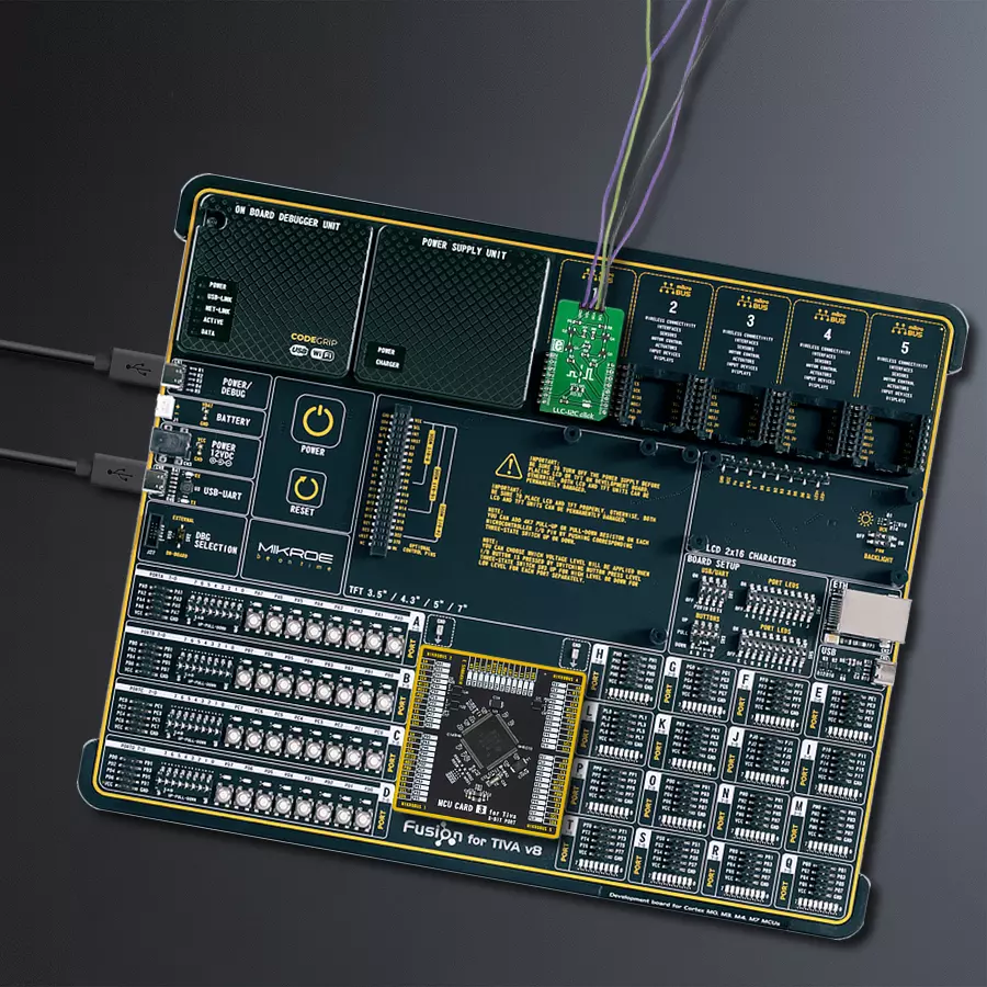
Dev. board
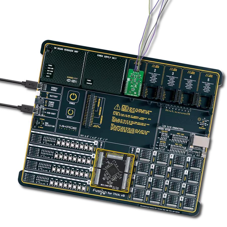
Fusion for Tiva v8
Compiler
NECTO Studio
MCU
TM4C129ENCPDT
Empower your projects with the ability to seamlessly convert logic levels between I2C devices, optimizing communication, reducing compatibility issues, and simplifying the integration of components with varying voltage thresholds
A
A
Hardware Overview
How does it work?
LLC-I2C Click does not use an integrated circuit, as already mentioned. With ICs avoided completely, there are some benefits gained: the overall cost of the LLC circuit is greatly reduced, a more robust MOSFET solution reduces the failure rate, and when powered off, both the low voltage and the high voltage sides are isolated from one another (by non-conductive MOSFETs). This type of circuit is sometimes referred to as a level shifting or level translating circuit and it is often necessary when the I2C slave device (typically a sensor IC) uses different logic voltage levels for the I2C communication than the master device, which is a host microcontroller in most cases. The conversion of this circuitry is bi-directional, which makes it suitable to be used with the I2C communication protocol. The I2C protocol was first introduced by NXP Semiconductors (formerly Philips Semiconductors), in 1982. They also introduced
an application note that explains the operation of the LLC circuit in more details. The circuit is divided into low-side and high-side sections for future reference, although the circuit is symmetrical and can be used in both directions. When there is no communication going on, both gates and sources of the MOSFETs are pulled up to their specific reference voltage levels. This will turn OFF both MOSFETs since there is no gate-source voltage difference (e.g. VG=VS=VSL). Since the I2C is operated by asserting its bus lines to a LOW logic level, when the source terminal of the MOSFET on one side (e.g. high-side) is driven to a LOW logic level, its VGS potential will rise since the gate voltage is fixed. When the VGS reaches the threshold voltage (1.2V typically for the used transistors), the MOSFET will turn ON, conducting current through the body diode of the opposite-side (low-side) MOSFET, which will become
directly polarized. This mechanism can be used to convert signal levels in both directions, within the whole operating range of the used MOSFETs. The reference voltage for the high-side can be selected by using the SMD jumper labeled as VCC SEL. The pull-up voltage for the high-side can be selected from the mikroBUS™ power rails, so it can be either 3.3V or 5V. For the low-side, an arbitrary reference voltage can be applied to the VSL pin of the J1 header, respecting the maximum voltage rating. J1 is the standard, 2.54mm pin-header. The low-side I2C bus pins are also routed to the J1 header, allowing an external device to be connected (using the standard wire-jumpers). As already mentioned, the low-side can actually use higher voltage levels than the master, but in most usage scenarios, it will be lower than the master, thus the terminology.


Features overview
Development board
Fusion for TIVA v8 is a development board specially designed for the needs of rapid development of embedded applications. It supports a wide range of microcontrollers, such as different 32-bit ARM® Cortex®-M based MCUs from Texas Instruments, regardless of their number of pins, and a broad set of unique functions, such as the first-ever embedded debugger/programmer over a WiFi network. The development board is well organized and designed so that the end-user has all the necessary elements, such as switches, buttons, indicators, connectors, and others, in one place. Thanks to innovative manufacturing technology, Fusion for TIVA v8 provides a fluid and immersive working experience, allowing access
anywhere and under any circumstances at any time. Each part of the Fusion for TIVA v8 development board contains the components necessary for the most efficient operation of the same board. An advanced integrated CODEGRIP programmer/debugger module offers many valuable programming/debugging options, including support for JTAG, SWD, and SWO Trace (Single Wire Output)), and seamless integration with the Mikroe software environment. Besides, it also includes a clean and regulated power supply module for the development board. It can use a wide range of external power sources, including a battery, an external 12V power supply, and a power source via the USB Type-C (USB-C) connector.
Communication options such as USB-UART, USB HOST/DEVICE, CAN (on the MCU card, if supported), and Ethernet is also included. In addition, it also has the well-established mikroBUS™ standard, a standardized socket for the MCU card (SiBRAIN standard), and two display options for the TFT board line of products and character-based LCD. Fusion for TIVA v8 is an integral part of the Mikroe ecosystem for rapid development. Natively supported by Mikroe software tools, it covers many aspects of prototyping and development thanks to a considerable number of different Click boards™ (over a thousand boards), the number of which is growing every day.

Microcontroller Overview
MCU Card / MCU
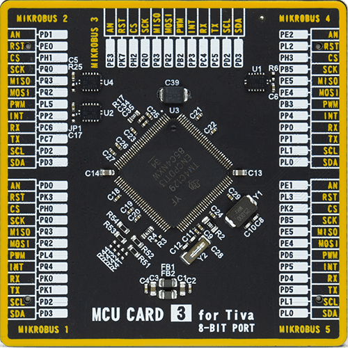
Type
8th Generation
Architecture
ARM Cortex-M4
MCU Memory (KB)
1024
Silicon Vendor
Texas Instruments
Pin count
128
RAM (Bytes)
262144
Used MCU Pins
mikroBUS™ mapper
Take a closer look
Click board™ Schematic

Step by step
Project assembly

Start by selecting your development board and Click board™. Begin with the Fusion for Tiva v8 as your development board.


Track your results in real time
Application Output
1. Application Output - In Debug mode, the 'Application Output' window enables real-time data monitoring, offering direct insight into execution results. Ensure proper data display by configuring the environment correctly using the provided tutorial.

2. UART Terminal - Use the UART Terminal to monitor data transmission via a USB to UART converter, allowing direct communication between the Click board™ and your development system. Configure the baud rate and other serial settings according to your project's requirements to ensure proper functionality. For step-by-step setup instructions, refer to the provided tutorial.

3. Plot Output - The Plot feature offers a powerful way to visualize real-time sensor data, enabling trend analysis, debugging, and comparison of multiple data points. To set it up correctly, follow the provided tutorial, which includes a step-by-step example of using the Plot feature to display Click board™ readings. To use the Plot feature in your code, use the function: plot(*insert_graph_name*, variable_name);. This is a general format, and it is up to the user to replace 'insert_graph_name' with the actual graph name and 'variable_name' with the parameter to be displayed.

Software Support
Library Description
This library contains API for LLC-I2C Click driver.
Key functions:
llci2c_generic_write- This function writes data to the desired registerllci2c_generic_read- This function reads data from the desired register
Open Source
Code example
The complete application code and a ready-to-use project are available through the NECTO Studio Package Manager for direct installation in the NECTO Studio. The application code can also be found on the MIKROE GitHub account.
/*!
 * \file
 * \brief LlcI2c Click example
 *
 * # Description
 * This Click can be utilized as the level converter for logic signals. The topology of this
 * logic level conversion (LLC) circuit is perfectly suited for the bi-directional I2C communication.
 *
 * The demo application is composed of two sections :
 *
 * ## Application Init
 * Initialization driver init
 *
 * ## Application Task
 * Reads the temperature from the Thermo 7 Click board and logs data to UART.
 *
 * *note:*
 * <pre>
 * Connection between Thermo 7 and I2C-LLC is made through I2C interface.
 * You can connect a Thermo 7 Click and I2C-LLC Click with the wires to make connection between Click boards.
 * We use the Thermo 7 Click to demonstrate the functions of the I2C-LLC Click.
 * </pre>
 *
 * \author MikroE Team
 *
 */
// ------------------------------------------------------------------- INCLUDES

#include "board.h"
#include "log.h"
#include "llci2c.h"

// ------------------------------------------------------------------ VARIABLES

static llci2c_t llci2c;
static log_t logger;

// ------------------------------------------------------ APPLICATION FUNCTIONS

void application_init ( void )
{
    log_cfg_t log_cfg;
    llci2c_cfg_t cfg;

    /**
     * Logger initialization.
     * Default baud rate: 115200
     * Default log level: LOG_LEVEL_DEBUG
     * @note If USB_UART_RX and USB_UART_TX
     * are defined as HAL_PIN_NC, you will
     * need to define them manually for log to work.
     * See @b LOG_MAP_USB_UART macro definition for detailed explanation.
     */
    LOG_MAP_USB_UART( log_cfg );
    log_init( &logger, &log_cfg );
    log_info( &logger, "---- Application Init ----" );

    //  Click initialization.

    llci2c_cfg_setup( &cfg );
    LLCI2C_MAP_MIKROBUS( cfg, MIKROBUS_1 );
    llci2c_init( &llci2c, &cfg );
}

void application_task ( void )
{
    // Thermo 7 measurement Temperature
    uint8_t write_reg = 0x00;
    uint8_t read_reg[ 2 ] = { 0 };

    float temp_msb;
    uint8_t temp_lsb;

    llci2c_generic_read ( &llci2c, write_reg, read_reg, 2 );

    temp_msb = read_reg[ 0 ];
    temp_lsb = read_reg[ 1 ] & 0xF0;

    if ( temp_lsb & 0x80 ) temp_msb += 0.50;
    if ( temp_lsb & 0x40 ) temp_msb += 0.25;
    if ( temp_lsb & 0x20 ) temp_msb += 0.125;
    if ( temp_lsb & 0x10 ) temp_msb += 0.0625;

    log_info( &logger, " Ambient temperature : %.2f C", temp_msb );
    Delay_ms ( 1000 );
}

int main ( void )
{
    /* Do not remove this line or clock might not be set correctly. */
    #ifdef PREINIT_SUPPORTED
    preinit();
    #endif

    application_init( );

    for ( ; ; )
    {
        application_task( );
    }

    return 0;
}


// ------------------------------------------------------------------------ END