Make cutting-edge A/D conversion with LTC2500-32 and TM4C1299NCZAD
Seamless transition, superior accuracy

Published Jun 08, 2023
Click board™
ADC 7 Click
Dev. board
Fusion for Tiva v8
Compiler
NECTO Studio
MCU
TM4C1299NCZAD
Enhance the performance of your designs with the power of our Analog-To-Digital converter
A
A
Hardware Overview
How does it work?
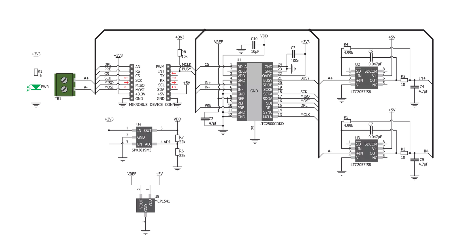
ADC 7 Click is based on the LTC2500-32, a 32-bit oversampling ADC with a configurable digital filter from Analog Devices. The integrated configurable filter is used to process the data from the 32-bit successive approximation register (SAR) core, providing a very low noise on the output, with a high dynamic range of up to 148dB. It also simplifies the design, as it relaxes anti-aliasing filter requirements for the input signal. The LTC2500-32 ADC also allows external reference voltage; therefore, the Click board™ uses 4.096V from a tiny fixed reference voltage IC from Microchip, the MCP1541. There is a two-pole screw terminal on the Click board™, with its inputs routed to the +IN and -IN pins of the ADC IC. The input signal can be bipolar, unipolar, or differential, swinging from 0 to VREF. Inputs are buffered with two LTC2057 operational amplifiers. These low-noise op-amps adjust the input impedance, as the LTC2500-32 ADC performs optimally when driven with low-impedance sources. The inputs are DC coupled - no decoupling capacitors are used on the input signal path. The LTC2500-32 has two SDO pins available (dual SPI interface), yet only SDOA pin is used on this Click board™, offering conversion data from the programmable digital filter. The RDLA pin should be set to a LOW logic level to initiate the SPI communication. It is routed to the CS pin of the mikroBUS™, while the SDOA pin is routed to the MISO pin of the mikroBUS™, labeled as SDO. Configured like this, it is possible to use the standard
four-pin SPI interface of the mikroBUS™ to communicate with the Click board™. The digital filter can be programmed via the SPI interface (SDI pin of the mikroBUS™), or it can use the PRE pin of the ADC IC. When the PRE pin is set to a HIGH logic level, a logic state on the SDI pin will be used to select one of two filters presets. Otherwise, the filter can be configured via the SPI interface when the PRE pin is set to a LOW logic level. PRE pin is routed to the RST pin of the mikroBUS™ and labeled as PRE. This IC uses an external signal to initiate the conversion process. The internal conversion process starts when a rising edge appears on the MCLK pin. For optimal performance, the manufacturer recommends that the external signal pulse duration should be 40nS. The MCLK pin is routed to the PWM pin of the mikroBUS™ and is labeled as MCK. After a rising edge on the MCLK pin, the ADC starts sampling by comparing the input voltage with the binary-weighted fractions of the reference voltage. The sampled input is then passed through the successive approximation algorithm (SAR ADC type). The conversion data comprises 24 bits for the differential voltage, 7 bits for the common mode voltage, and one flag bit used as a signal overflow indicator (VIN > VREF). This data is then passed to the filter section, which stores a 32-bit processed value on the output register. The ADC IC compares the differential input voltage with the 2 × VREF, divided into 232 levels, resulting in a 1.9mV resolution (using 4.096V as a reference).
The wide common-mode input range (from 0V up to VREF), coupled with the high common-mode rejection rate, allows all types of signals to be sampled by the device: pseudo-differential unipolar, pseudo-differential bipolar, and fully differential. It is a unique feature of the LTC2500-32 ADC device. During the conversion phase, the BUSY pin is kept at the HIGH logic level (Hi-Z). This pin is driven to a LOW logic level when the conversion ends. The BUSY pin indicates the conversion-in-progress state and is routed to the mikroBUS™ INT pin, labeled as BSY. Another pin of the LTC2500-32 ADC with a similar function indicates that data is ready to be read at the output register. This pin is labeled as DRL and routed to the mikroBUS™ AN pin. By using these pins as the interrupt sources, the host MCU can achieve optimized data acquisition timing, not having to poll the ADC until it gets ready. The Click board™ uses both 3.3V and 5V rails of the mikroBUS™.The 3.3V rail provides the operating voltage for the ADC IC, which is 2.5V. Therefore, a small LDO is used to obtain this voltage. The 5V rail of the mikroBUS™ is used as the input voltage for the MCP1541 reference voltage source. Since the logic section of the LTC2500-32 ADC can operate with voltages from 1.8V up to 5V, no additional communication level shifting ICs are required, and the Click board™ can operate with both 3.3V and 5V MCUs.

Features overview
Development board
Fusion for TIVA v8 is a development board specially designed for the needs of rapid development of embedded applications. It supports a wide range of microcontrollers, such as different 32-bit ARM® Cortex®-M based MCUs from Texas Instruments, regardless of their number of pins, and a broad set of unique functions, such as the first-ever embedded debugger/programmer over a WiFi network. The development board is well organized and designed so that the end-user has all the necessary elements, such as switches, buttons, indicators, connectors, and others, in one place. Thanks to innovative manufacturing technology, Fusion for TIVA v8 provides a fluid and immersive working experience, allowing access
anywhere and under any circumstances at any time. Each part of the Fusion for TIVA v8 development board contains the components necessary for the most efficient operation of the same board. An advanced integrated CODEGRIP programmer/debugger module offers many valuable programming/debugging options, including support for JTAG, SWD, and SWO Trace (Single Wire Output)), and seamless integration with the Mikroe software environment. Besides, it also includes a clean and regulated power supply module for the development board. It can use a wide range of external power sources, including a battery, an external 12V power supply, and a power source via the USB Type-C (USB-C) connector.
Communication options such as USB-UART, USB HOST/DEVICE, CAN (on the MCU card, if supported), and Ethernet is also included. In addition, it also has the well-established mikroBUS™ standard, a standardized socket for the MCU card (SiBRAIN standard), and two display options for the TFT board line of products and character-based LCD. Fusion for TIVA v8 is an integral part of the Mikroe ecosystem for rapid development. Natively supported by Mikroe software tools, it covers many aspects of prototyping and development thanks to a considerable number of different Click boards™ (over a thousand boards), the number of which is growing every day.

Microcontroller Overview
MCU Card / MCU
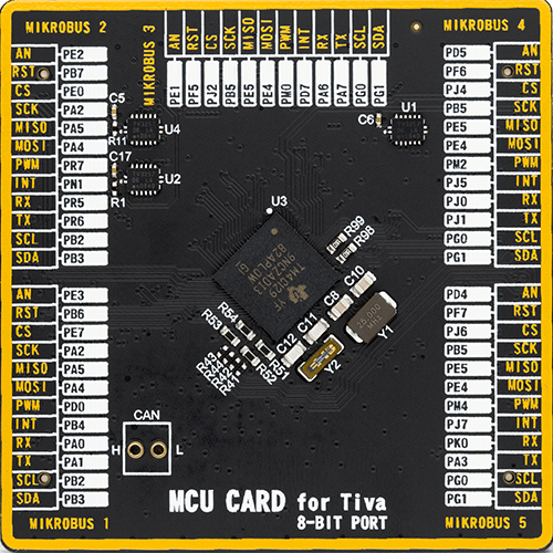
Type
8th Generation
Architecture
ARM Cortex-M4
MCU Memory (KB)
1024
Silicon Vendor
Texas Instruments
Pin count
212
RAM (Bytes)
262144
Used MCU Pins
mikroBUS™ mapper
Take a closer look
Click board™ Schematic
Step by step
Project assembly

Start by selecting your development board and Click board™. Begin with the Fusion for Tiva v8 as your development board.


Software Support
Library Description
This library contains API for ADC 7 Click driver.
Key functions:
adc7_set_configFunction performs the device configuration by sending configuration dataadc7_start_conv_cycleFunction generates clock signal on MCK pin and on that way starts conversionadc7_read_resultsFunction reads voltage value from AD converter and calculates this value to mV
Open Source
Code example
The complete application code and a ready-to-use project are available through the NECTO Studio Package Manager for direct installation in the NECTO Studio. The application code can also be found on the MIKROE GitHub account.
/*!
 * \file
 * \brief ADC7 Click example
 *
 * # Description
 * This application collects data from the analog signal, calculates and logs the
 * converted voltage value.
 *
 * The demo application is composed of two sections :
 *
 * ## Application Init
 * Initializes driver and performs configuration for conversion cycles.
 *
 * ## Application Task
 * Performs the determined number of conversion cycles which are necessary for averaging.
 * When all conversion cycles are done, it reads the converted voltage value.
 * Results will be logged on UART terminal every second.
 *
 * \author MikroE Team
 *
 */
// ------------------------------------------------------------------- INCLUDES

#include "board.h"
#include "log.h"
#include "adc7.h"

// ------------------------------------------------------------------ VARIABLES

static adc7_t adc7;
static log_t logger;

static float voltage_data;

// ------------------------------------------------------ APPLICATION FUNCTIONS

void application_init ( void )
{
    log_cfg_t log_cfg;
    adc7_cfg_t cfg;

    /**
     * Logger initialization.
     * Default baud rate: 115200
     * Default log level: LOG_LEVEL_DEBUG
     * @note If USB_UART_RX and USB_UART_TX
     * are defined as HAL_PIN_NC, you will
     * need to define them manually for log to work.
     * See @b LOG_MAP_USB_UART macro definition for detailed explanation.
     */
    LOG_MAP_USB_UART( log_cfg );
    log_init( &logger, &log_cfg );
    log_info( &logger, "---- Application Init ----" );
    Delay_ms ( 100 );

    //  Click initialization.

    adc7_cfg_setup( &cfg );
    ADC7_MAP_MIKROBUS( cfg, MIKROBUS_1 );
    adc7_init( &adc7, &cfg );

    adc7_default_cfg( &adc7 );
}

void application_task ( void )
{
    adc7_start_conv_cycle( &adc7 );
    adc7_read_results( &adc7, &voltage_data );
    log_printf( &logger, "Voltage: %.2f mV\r\n", voltage_data );

    Delay_ms ( 1000 );
}

int main ( void )
{
    /* Do not remove this line or clock might not be set correctly. */
    #ifdef PREINIT_SUPPORTED
    preinit();
    #endif

    application_init( );

    for ( ; ; )
    {
        application_task( );
    }

    return 0;
}

// ------------------------------------------------------------------------ END


