Charge up and be ready with LTC3225 and STM32L496AG
Reliable power, uninterrupted performance
Published Jul 22, 2025
Click board™
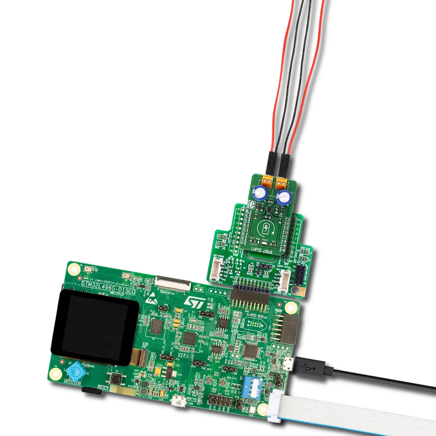
UPS Click
Dev. board
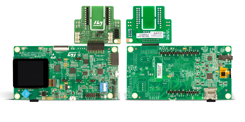
Discovery kit with STM32L496AG MCU
Compiler
NECTO Studio
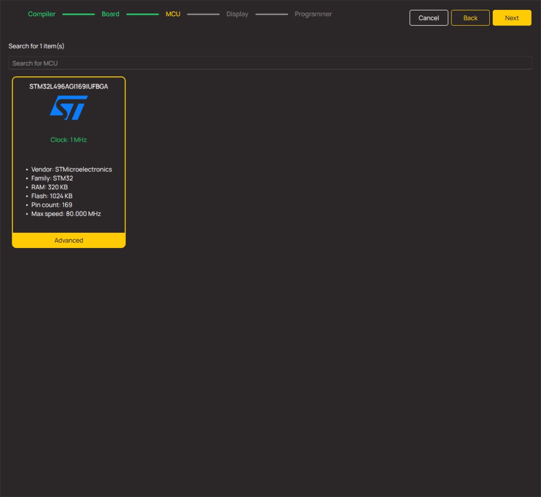
MCU
STM32L496AG
Say goodbye to slow charging and unreliable power sources - experience seamless operations with our ultimate UPS solution
A
A
Hardware Overview
How does it work?
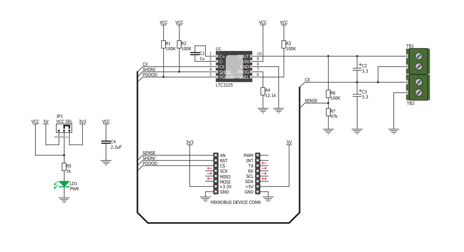
UPS Click is based on the LTC3225, a 150mA supercapacitor charger from Analog Devices, used to charge two serially connected capacitors with a controlled current and constant voltage. The LTC3225 has the unique ability to maintain constant voltage levels on both of the connected supercapacitors by monitoring their voltages. This improves the lifecycle of the supercapacitors, protecting them from overvoltage. When a voltage difference occurs during charging (depending on the dissimilarities between the two used supercapacitors), the voltage across one of them might rise enough to cause damage. Unlike other balancing techniques that use resistors to discharge the capacitor, which has a greater voltage, the LTC3225 automatically adjusts the charging currents of two capacitors until their charging speed is equal. The difference between the charging currents can be increased or decreased by 50%. When the Cout voltage reaches its nominal value (selected by the pull-up resistor on the Vsel pin to 5.3V), the internal charge pump is turned off, allowing the IC to enter the low power mode. The recharging cycle is automatically restarted when the voltage of the supercapacitors drops under a threshold. The output terminals are used to connect an external load. There are two screw terminals routed to the output pins of each capacitor. Two supercapacitors are serially connected: the high-side capacitor has its positive pin connected to the Cout (a regulated voltage output pin),
while the low-side capacitor has its negative pin connected to the GND. The negative pin of the high-side supercapacitor and the positive pin of the low-side supercapacitor are connected together and routed to the CX pin of the LTC3225, which is maintained at Cout/2. Therefore, the voltage across a single terminal is Cout/2, so to use the full range of the output voltage, a load should be connected between the high-side terminal labeled with the “+” sign and the low-side terminal labeled with the “-” sign. These terminals can also be used to connect additional supercapacitors since the supercapacitors are in parallel with the connected load. When the power source is turned off, the output voltage (Cout) depends only on used supercapacitors. These two supercapacitors have an equivalent capacitance of 1.65F, and they will become the only elements that provide power for the connected load when the power supply is removed. According to the capacitor discharging formula, these capacitors will discharge through the connected load, and the output voltage will exponentially decrease. The #SHDN pin can put the device in the low-power shutdown mode by applying a LOW logic level. This pin is routed to the RST pin of the mikroBUS™, labeled as SDN. It is pulled to a HIGH logic level by an onboard pull-up resistor. It is possible to read the output voltage value by using the voltage divider connected between the GND and the Cout. When the supercapacitors are fully charged, with the Cout
voltage level of 5.3V, the value on the middle point of the voltage divider will be about 1.7V. The middle point of the voltage divider is routed to the AN pin of the mikroBUS™, allowing an easy analog-to-digital conversion by the host MCU. This pin is labeled as SEN on the Click board™. The PGOOD pin of LTC3225 IC is routed to the mikroBUS™ CS pin and labeled as PGD. This pin is an open-drain output, and it is pulled to a HIGH logic level by an onboard resistor. When the output voltage reaches a value 6% below the nominal value, this pin is de-asserted. When the voltage drops under 7.2% below its nominal value, this pin is asserted and pulled to a LOW logic level. It can be used to monitor the state of the output supercapacitors. The Click board™ uses a power supply from the mikroBUS™. Moving the onboard SMD jumper labeled JP1 makes it possible to select either a 3.3V or 5V rail as the input power source. It also selects the IC operating voltage, allowing interfacing with both the 5V and 3.3V MCUs. Regardless of the selected operating voltage, the output voltage is always 5.3V, as set by the Vsel pin of the UPS click. UPS click uses only the GPIO pins of the MCU for setting states on its pins; therefore, it is extremely easy to work with. However, the Click board™ comes equipped with a library containing easy-to-use functions and an example code that can be used, as a reference, for further development.

Features overview
Development board
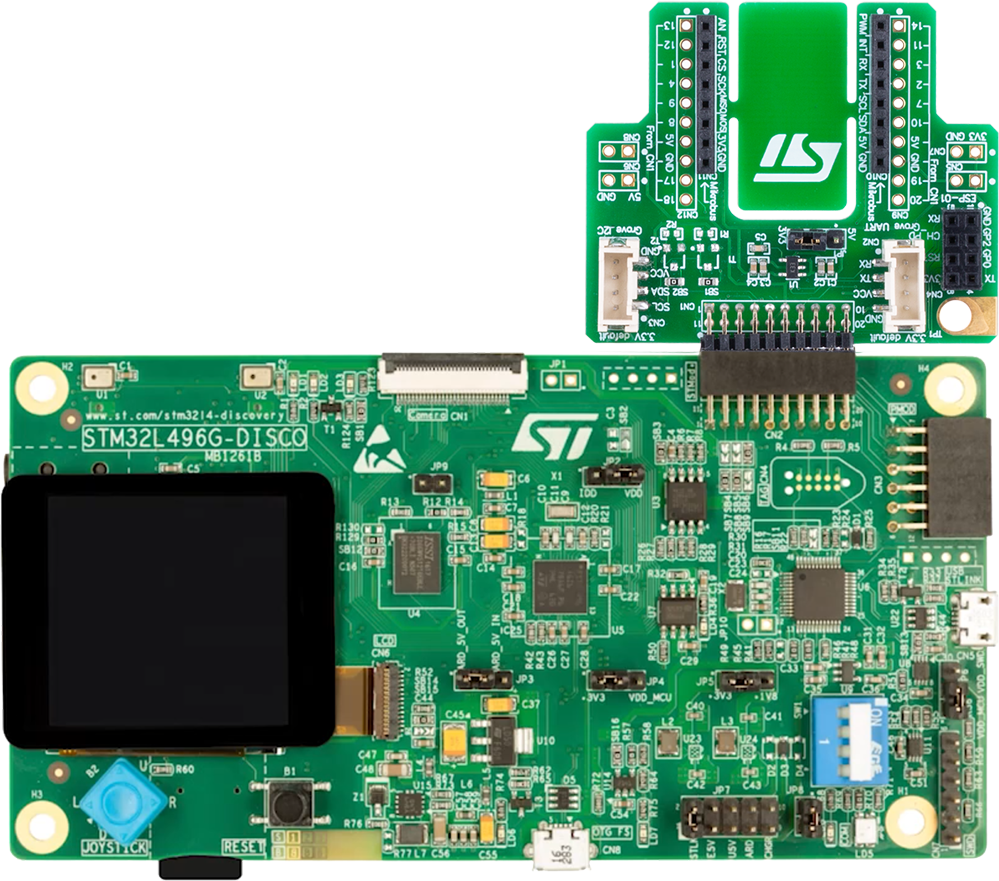
The 32L496GDISCOVERY Discovery kit serves as a comprehensive demonstration and development platform for the STM32L496AG microcontroller, featuring an Arm® Cortex®-M4 core. Designed for applications that demand a balance of high performance, advanced graphics, and ultra-low power consumption, this kit enables seamless prototyping for a wide range of embedded solutions. With its innovative energy-efficient
architecture, the STM32L496AG integrates extended RAM and the Chrom-ART Accelerator, enhancing graphics performance while maintaining low power consumption. This makes the kit particularly well-suited for applications involving audio processing, graphical user interfaces, and real-time data acquisition, where energy efficiency is a key requirement. For ease of development, the board includes an onboard ST-LINK/V2-1
debugger/programmer, providing a seamless out-of-the-box experience for loading, debugging, and testing applications without requiring additional hardware. The combination of low power features, enhanced memory capabilities, and built-in debugging tools makes the 32L496GDISCOVERY kit an ideal choice for prototyping advanced embedded systems with state-of-the-art energy efficiency.
Microcontroller Overview
MCU Card / MCU
Architecture
ARM Cortex-M4
MCU Memory (KB)
1024
Silicon Vendor
STMicroelectronics
Pin count
169
RAM (Bytes)
327680
Used MCU Pins
mikroBUS™ mapper
Take a closer look
Click board™ Schematic
Step by step
Project assembly
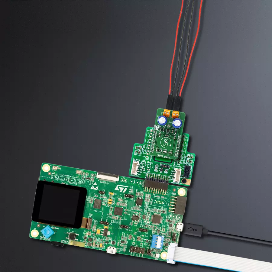
Start by selecting your development board and Click board™. Begin with the Discovery kit with STM32L496AG MCU as your development board.


Track your results in real time
Application Output
1. Application Output - In Debug mode, the 'Application Output' window enables real-time data monitoring, offering direct insight into execution results. Ensure proper data display by configuring the environment correctly using the provided tutorial.

2. UART Terminal - Use the UART Terminal to monitor data transmission via a USB to UART converter, allowing direct communication between the Click board™ and your development system. Configure the baud rate and other serial settings according to your project's requirements to ensure proper functionality. For step-by-step setup instructions, refer to the provided tutorial.

3. Plot Output - The Plot feature offers a powerful way to visualize real-time sensor data, enabling trend analysis, debugging, and comparison of multiple data points. To set it up correctly, follow the provided tutorial, which includes a step-by-step example of using the Plot feature to display Click board™ readings. To use the Plot feature in your code, use the function: plot(*insert_graph_name*, variable_name);. This is a general format, and it is up to the user to replace 'insert_graph_name' with the actual graph name and 'variable_name' with the parameter to be displayed.

Software Support
Library Description
This library contains API for UPS Click driver.
Key functions:
usp_set_mode- Functions for settings chip modeups_get_power_good- Functions for reading PGD state
Open Source
Code example
The complete application code and a ready-to-use project are available through the NECTO Studio Package Manager for direct installation in the NECTO Studio. The application code can also be found on the MIKROE GitHub account.
/*!
 * \file
 * \brief UPS Click example
 *
 * # Description
 * This application is charger, that provides continuous power for a load connected to the output terminals.
 *
 * The demo application is composed of two sections :
 *
 * ## Application Init
 * Initializes Driver init and setting chip mode as ACTIVE
 *
 * ## Application Task
 * Checks the state of PGD (Power Good), PGD goes high when Vout is within 6% of target value (4.98V)
 *
 * \author MikroE Team
 *
 */
// ------------------------------------------------------------------- INCLUDES

#include "board.h"
#include "log.h"
#include "ups.h"

// ------------------------------------------------------------------ VARIABLES

static ups_t ups;
static log_t logger;

// ------------------------------------------------------ APPLICATION FUNCTIONS

void application_init ( void )
{
    log_cfg_t log_cfg;
    ups_cfg_t cfg;

    /**
     * Logger initialization.
     * Default baud rate: 115200
     * Default log level: LOG_LEVEL_DEBUG
     * @note If USB_UART_RX and USB_UART_TX
     * are defined as HAL_PIN_NC, you will
     * need to define them manually for log to work.
     * See @b LOG_MAP_USB_UART macro definition for detailed explanation.
     */
    LOG_MAP_USB_UART( log_cfg );
    log_init( &logger, &log_cfg );
    log_info(&logger, "---- Application Init ----");

    //  Click initialization.

    ups_cfg_setup( &cfg );
    UPS_MAP_MIKROBUS( cfg, MIKROBUS_1 );
    ups_init( &ups, &cfg );

    usp_set_mode( &ups, UPS_MODE_ACTIVE );
}

void application_task ( )
{
    uint8_t pgd_state;

    pgd_state = ups_get_power_good( &ups );

    if ( pgd_state != 0 )
    {
        log_printf( &logger, "---> Power Good \r\n" );
    }
    Delay_1sec( );
}

int main ( void )
{
    /* Do not remove this line or clock might not be set correctly. */
    #ifdef PREINIT_SUPPORTED
    preinit();
    #endif

    application_init( );

    for ( ; ; )
    {
        application_task( );
    }

    return 0;
}

// ------------------------------------------------------------------------ END
Additional Support
Resources
Category:Battery charger