Empower your devices with bespoke power using MAX17572 and PIC18F65K40
Voltage control made easy

Published Nov 30, 2024
Click board™
Buck 6 Click
Dev. board
UNI-DS v8
Compiler
NECTO Studio
MCU
PIC18F65K40
With its voltage regulation capabilities, this step-down buck solution ensures your electronic circuits' stable and reliable operation
A
A
Hardware Overview
How does it work?
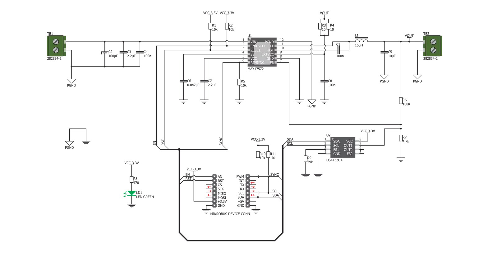
Buck 6 Click is based on the MAX17572, a step-down (buck) DC-DC converter from Analog Devices. This IC is the primary voltage regulation component, used in conjunction with the DS4432U, a dual channel, 7-Bit digital-to-analog converter (DAC) with the I2C interface, also from Analog Devices. The DAC is connected to the FB pin of the MAX17572, affecting its internal PWM duty cycle and changing the output voltage that way. The MAX17572 requires very few components allowing the clean and simple design of the final application, considering all its features. The MAX17572 features robust overload and short-circuit protection. When the internally set current limit of 1.7A is exceeded, the high-side MOSFET is turned off, and the hiccup mode is triggered. This mode suspends the operation for 32,768 duty cycles, after which the soft start sequence is reattempted. If the fault condition is still present and the feedback voltage remains under 0.58V, the switching frequency will be halved to avoid overheating during the restart sequence. The output voltage regulation ranges from 0.9V up to 20V, with the input voltage up to 30V and greater than 5V. It should be noted that the input voltage must always be greater than the desired output
voltage. The voltage can be set via the I2C interface of the DS4432U DAC. The DAC is powered by the 3.3V rail of the mikroBUS™. This DAC requires very few components, such as the full-scale selection resistor. Since only one channel of the DAC is used, even fewer components are required for DAC itself. The DAC can both source and sink the current, so it must be properly set to get the desired effect on the output voltage. The included click board™ library contains a function that sets all the required initialization parameters and functions used to set up the output voltage. The soft start feature prevents the inrush current. The soft start capacitor determines this feature. The soft start is set to about 10ms on the BUCK 6 click. The EN pin of the MAX17572 is routed to the AN pin of the mikroBUS™. This pin is used to enable the buck converter but can also be used to set the undervoltage lockout threshold. If the input voltage falls under this threshold, the internal low drop output regulators (LDOs) will not power on the internal logic, and the buck converter will stay disabled. The onboard resistor pulls the EN pin up to the 3.3V mikroBUS™ power rail. The #RESET pin of the MAX17572 is an open drain output, and it is pulled to a HIGH logic level
by the onboard resistor. This pin is routed to the RST pin of the mikroBUS™ and can be used as the power good indication. When the output voltage drops below 92% of the nominal regulated output voltage, this pin is asserted and driven to a LOW logic level. One of the distinctive features of this buck converter is the ability to synchronize the switching clock frequency with an external clock signal. It is possible to synchronize the switching frequency within a range of about 0% to 10% lower than the value set by the onboard resistor, which is about 1.8MHz. For synchronizing purposes, the SYNC pin is routed to the PWM pin of the mikroBUS™. This feature primarily synchronizes switching frequencies when more than a single buck converter is used. The Click board™ is equipped with two screw terminals for an easy and secure connection. The input terminal is used to connect the input power source, while the output terminal is used to connect the load up to 1A. The click board is supplied with the auxiliary power for the DAC and other logic sections of the click board from the mikroBUS™ 3.3V power rail.

Features overview
Development board
UNI-DS v8 is a development board specially designed for the needs of rapid development of embedded applications. It supports a wide range of microcontrollers, such as different STM32, Kinetis, TIVA, CEC, MSP, PIC, dsPIC, PIC32, and AVR MCUs regardless of their number of pins, and a broad set of unique functions, such as the first-ever embedded debugger/programmer over WiFi. The development board is well organized and designed so that the end-user has all the necessary elements, such as switches, buttons, indicators, connectors, and others, in one place. Thanks to innovative manufacturing technology, UNI-DS v8 provides a fluid and immersive working experience, allowing access anywhere and under any
circumstances at any time. Each part of the UNI-DS v8 development board contains the components necessary for the most efficient operation of the same board. An advanced integrated CODEGRIP programmer/debugger module offers many valuable programming/debugging options, including support for JTAG, SWD, and SWO Trace (Single Wire Output)), and seamless integration with the Mikroe software environment. Besides, it also includes a clean and regulated power supply module for the development board. It can use a wide range of external power sources, including a battery, an external 12V power supply, and a power source via the USB Type-C (USB-C) connector. Communication options such as USB-UART, USB
HOST/DEVICE, CAN (on the MCU card, if supported), and Ethernet is also included. In addition, it also has the well-established mikroBUS™ standard, a standardized socket for the MCU card (SiBRAIN standard), and two display options for the TFT board line of products and character-based LCD. UNI-DS v8 is an integral part of the Mikroe ecosystem for rapid development. Natively supported by Mikroe software tools, it covers many aspects of prototyping and development thanks to a considerable number of different Click boards™ (over a thousand boards), the number of which is growing every day.

Microcontroller Overview
MCU Card / MCU

Type
8th Generation
Architecture
PIC (8-bit)
MCU Memory (KB)
32
Silicon Vendor
Microchip
Pin count
64
RAM (Bytes)
2048
Used MCU Pins
mikroBUS™ mapper
Take a closer look
Click board™ Schematic
Step by step
Project assembly

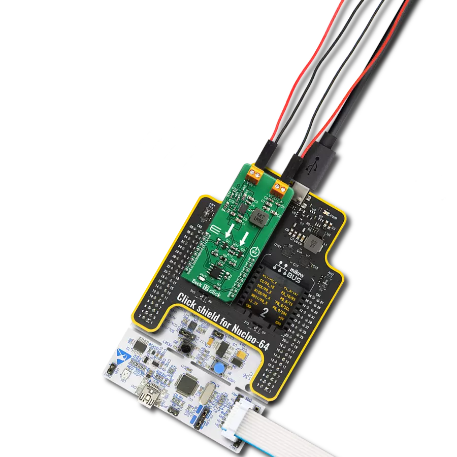
Start by selecting your development board and Click board™. Begin with the UNI-DS v8 as your development board.


Track your results in real time
Application Output
1. Application Output - In Debug mode, the 'Application Output' window enables real-time data monitoring, offering direct insight into execution results. Ensure proper data display by configuring the environment correctly using the provided tutorial.

2. UART Terminal - Use the UART Terminal to monitor data transmission via a USB to UART converter, allowing direct communication between the Click board™ and your development system. Configure the baud rate and other serial settings according to your project's requirements to ensure proper functionality. For step-by-step setup instructions, refer to the provided tutorial.

3. Plot Output - The Plot feature offers a powerful way to visualize real-time sensor data, enabling trend analysis, debugging, and comparison of multiple data points. To set it up correctly, follow the provided tutorial, which includes a step-by-step example of using the Plot feature to display Click board™ readings. To use the Plot feature in your code, use the function: plot(*insert_graph_name*, variable_name);. This is a general format, and it is up to the user to replace 'insert_graph_name' with the actual graph name and 'variable_name' with the parameter to be displayed.

Software Support
Library Description
This library contains API for Buck 6 Click driver.
Key functions:
buck6_get_rst- Gets resetbuck6_set_mode- Set modebuck6_set_max_voltage- Set maximum voltage
Open Source
Code example
The complete application code and a ready-to-use project are available through the NECTO Studio Package Manager for direct installation in the NECTO Studio. The application code can also be found on the MIKROE GitHub account.
/*!
 * \file
 * \brief BUCK6 Click example
 *
 * # Description
 * BUCK 6 Click is an advanced synchronous DC-DC step down (buck) converter,
 * with a very wide input voltage range and reasonably high output current.
 *
 * The demo application is composed of two sections :
 *
 * ## Application Init
 * Initialization Driver init and settings chip on ACTIVE mode and setting the maximum range to 5V.
 *
 * ## Application Task
 * Sets the different ranges of the maximum voltage.
 *
 *
 * \author MikroE Team
 *
 */
// ------------------------------------------------------------------- INCLUDES

#include "board.h"
#include "log.h"
#include "buck6.h"

// ------------------------------------------------------------------ VARIABLES

static buck6_t buck6;
static log_t logger;

void application_init ( void )
{
    log_cfg_t log_cfg;
    buck6_cfg_t cfg;

    /**
     * Logger initialization.
     * Default baud rate: 115200
     * Default log level: LOG_LEVEL_DEBUG
     * @note If USB_UART_RX and USB_UART_TX
     * are defined as HAL_PIN_NC, you will
     * need to define them manually for log to work.
     * See @b LOG_MAP_USB_UART macro definition for detailed explanation.
     */
    LOG_MAP_USB_UART( log_cfg );
    log_init( &logger, &log_cfg );
    log_info( &logger, "---- Application Init ----" );

    //  Click initialization.

    buck6_cfg_setup( &cfg );
    BUCK6_MAP_MIKROBUS( cfg, MIKROBUS_1 );
    buck6_init( &buck6, &cfg );

    buck6_set_mode( &buck6, BUCK6_ACTIVE_MODE );
    buck6_set_max_voltage( &buck6, BUCK6_MAX_RANGE_5000mV );
    Delay_ms ( 100 );
}

void application_task ( void )
{
    buck6_set_max_voltage( &buck6, BUCK6_MAX_RANGE_2500mV );
    Delay_ms ( 1000 );
    Delay_ms ( 1000 );
    Delay_ms ( 1000 );
    buck6_set_max_voltage( &buck6, BUCK6_MAX_RANGE_5000mV );
    Delay_ms ( 1000 );
    Delay_ms ( 1000 );
    Delay_ms ( 1000 );
    buck6_set_max_voltage( &buck6, BUCK6_MAX_RANGE_7500mV );
    Delay_ms ( 1000 );
    Delay_ms ( 1000 );
    Delay_ms ( 1000 );
    buck6_set_max_voltage( &buck6, BUCK6_MAX_RANGE_10000mV );
    Delay_ms ( 1000 );
    Delay_ms ( 1000 );
    Delay_ms ( 1000 );
    buck6_set_max_voltage( &buck6, BUCK6_MAX_RANGE_7500mV );
    Delay_ms ( 1000 );
    Delay_ms ( 1000 );
    Delay_ms ( 1000 );
    buck6_set_max_voltage( &buck6, BUCK6_MAX_RANGE_5000mV );
    Delay_ms ( 1000 );
    Delay_ms ( 1000 );
    Delay_ms ( 1000 );
}

int main ( void )
{
    /* Do not remove this line or clock might not be set correctly. */
    #ifdef PREINIT_SUPPORTED
    preinit();
    #endif

    application_init( );

    for ( ; ; )
    {
        application_task( );
    }

    return 0;
}


// ------------------------------------------------------------------------ END