Digitizes the input voltage with MAX22530 and STM32F411RE and transmits the data across the isolation barrier
Step into the future of data conversion

Published Jun 01, 2023
Click board™
ISO ADC 5 Click
Dev. board
Fusion for ARM v8
Compiler
NECTO Studio
MCU
STM32F411RE
Harness the power of isolation for accurate signal conversion with our A/D converter
A
A
Hardware Overview
How does it work?
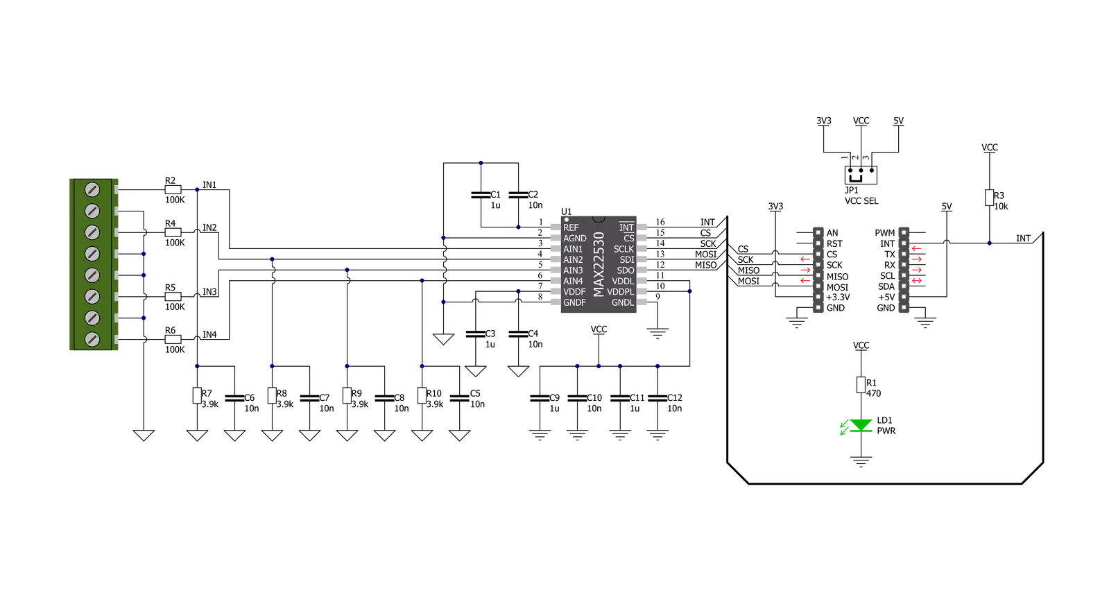
ISO ADC 5 Click is based on the MAX22530, a 12-bit, 4-channel ADC with a 5kVRMS isolated SPI interface from Analog Devices. The ADC and all field-side circuits are powered by an integrated, isolated DC-DC converter that can verify field-side functionality even when there is no input signal or other field-side supply. It continually digitizes the input voltage on the field side of an isolation barrier and transmits the data across the isolation barrier to the logic side of the devices, where the magnitude of the input voltage is compared to programmable thresholds. The MAX22530 ADC employs a 12-bit SAR architecture with a nominal sampling rate of 20ksps per channel and has an
input voltage of up to 1.8V. Placed voltage dividers make the proper ADC input voltage on the analog input channels, which, based on the input in the range from 0 to 48V, gives the required input to the ADC in its range from 0 to 1.8V. After Power-Up, the ADC runs continually at the nominal sampling rate. The MAX22530 also features a precision internal voltage reference of 1.8V with a maximum error of ±2% over the entire operating temperature range. The MAX22530 communicates with MCU using the standard SPI serial interface with a maximum frequency 10MHz. Besides, it continuously monitors multiple possible fault conditions such as ADC functionality error, SPI framing
error, CRC errors from SPI communications, and internal isolated data stream loss. This hardware alert feature is provided through the interrupt pin, routed on the CS pin of the mikroBUS™ socket, which asserts low when an enabled fault is detected. This Click board™ can operate with either 3.3V or 5V logic voltage levels selected via the VCC SEL jumper. This way, both 3.3V and 5V capable MCUs can use the communication lines properly. However, the Click board™ comes equipped with a library containing easy-to-use functions and an example code that can be used, as a reference, for further development.


Features overview
Development board
Fusion for ARM v8 is a development board specially designed for the needs of rapid development of embedded applications. It supports a wide range of microcontrollers, such as different ARM® Cortex®-M based MCUs regardless of their number of pins, and a broad set of unique functions, such as the first-ever embedded debugger/programmer over WiFi. The development board is well organized and designed so that the end-user has all the necessary elements, such as switches, buttons, indicators, connectors, and others, in one place. Thanks to innovative manufacturing technology, Fusion for ARM v8 provides a fluid and immersive working experience, allowing access anywhere and under any
circumstances at any time. Each part of the Fusion for ARM v8 development board contains the components necessary for the most efficient operation of the same board. An advanced integrated CODEGRIP programmer/debugger module offers many valuable programming/debugging options, including support for JTAG, SWD, and SWO Trace (Single Wire Output)), and seamless integration with the Mikroe software environment. Besides, it also includes a clean and regulated power supply module for the development board. It can use a wide range of external power sources, including a battery, an external 12V power supply, and a power source via the USB Type-C (USB-C) connector.
Communication options such as USB-UART, USB HOST/DEVICE, CAN (on the MCU card, if supported), and Ethernet is also included. In addition, it also has the well-established mikroBUS™ standard, a standardized socket for the MCU card (SiBRAIN standard), and two display options for the TFT board line of products and character-based LCD. Fusion for ARM v8 is an integral part of the Mikroe ecosystem for rapid development. Natively supported by Mikroe software tools, it covers many aspects of prototyping and development thanks to a considerable number of different Click boards™ (over a thousand boards), the number of which is growing every day.

Microcontroller Overview
MCU Card / MCU
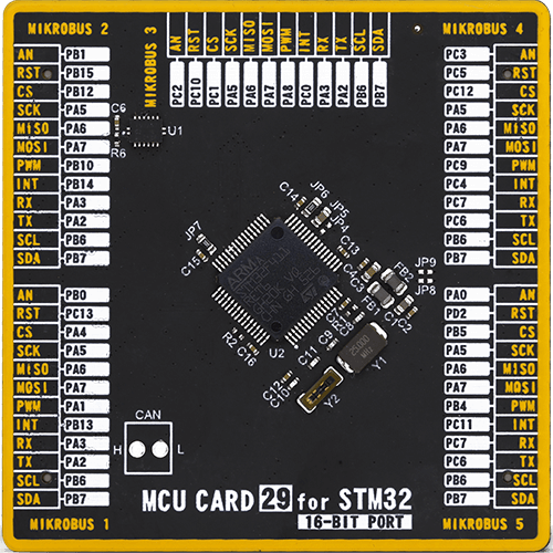
Type
8th Generation
Architecture
ARM Cortex-M4
MCU Memory (KB)
512
Silicon Vendor
STMicroelectronics
Pin count
64
RAM (Bytes)
131072
Used MCU Pins
mikroBUS™ mapper
Take a closer look
Click board™ Schematic
Step by step
Project assembly

Start by selecting your development board and Click board™. Begin with the Fusion for ARM v8 as your development board.


Software Support
Library Description
This library contains API for ISO ADC 5 Click driver.
Key functions:
isoadc5_cfg_setup- Config Object Initialization function.isoadc5_init- Initialization function.
Open Source
Code example
The complete application code and a ready-to-use project are available through the NECTO Studio Package Manager for direct installation in the NECTO Studio. The application code can also be found on the MIKROE GitHub account.
/*!
 * @file main.c
 * @brief ISOADC5 Click example
 *
 * # Description
 * This example demonstrates the use of ISO ADC 5 Click board.
 *
 * The demo application is composed of two sections :
 *
 * ## Application Init
 * Initializes the driver and makes an initial log.
 *
 * ## Application Task
 * Reads the voltage from all input channels and displays the values of
 * each channel on the USB UART approximately every second.
 *
 * @note
 * The voltage input range is from 0 to 48V.
 *
 * @author Stefan Filipovic
 *
 */

#include "board.h"
#include "log.h"
#include "isoadc5.h"

static isoadc5_t isoadc5;
static log_t logger;

void application_init ( void )
{
    log_cfg_t log_cfg;          /**< Logger config object. */
    isoadc5_cfg_t isoadc5_cfg;  /**< Click config object. */

    /**
     * Logger initialization.
     * Default baud rate: 115200
     * Default log level: LOG_LEVEL_DEBUG
     * @note If USB_UART_RX and USB_UART_TX
     * are defined as HAL_PIN_NC, you will
     * need to define them manually for log to work.
     * See @b LOG_MAP_USB_UART macro definition for detailed explanation.
     */
    LOG_MAP_USB_UART( log_cfg );
    log_init( &logger, &log_cfg );
    Delay_ms ( 100 );
    log_info( &logger, " Application Init " );

    // Click initialization.
    isoadc5_cfg_setup( &isoadc5_cfg );
    ISOADC5_MAP_MIKROBUS( isoadc5_cfg, MIKROBUS_1 );
    err_t init_flag  = isoadc5_init( &isoadc5, &isoadc5_cfg );
    if ( SPI_MASTER_ERROR == init_flag )
    {
        log_error( &logger, " Application Init Error. " );
        log_info( &logger, " Please, run program again... " );

        for ( ; ; );
    }
    log_info( &logger, " Application Task " );
}

void application_task ( void )
{
    float v_ain1 = 0, v_ain2 = 0, v_ain3 = 0, v_ain4 = 0;
    err_t error_flag = isoadc5_read_voltage( &isoadc5, ISOADC5_ADC_FILTERED, ISOADC5_ADC_CHANNEL_1, &v_ain1 );
    error_flag |= isoadc5_read_voltage( &isoadc5, ISOADC5_ADC_FILTERED, ISOADC5_ADC_CHANNEL_2, &v_ain2 );
    error_flag |= isoadc5_read_voltage( &isoadc5, ISOADC5_ADC_FILTERED, ISOADC5_ADC_CHANNEL_3, &v_ain3 );
    error_flag |= isoadc5_read_voltage( &isoadc5, ISOADC5_ADC_FILTERED, ISOADC5_ADC_CHANNEL_4, &v_ain4 );

    if ( ISOADC5_OK == error_flag )
    {
        log_printf( &logger, " AIN 1 voltage: %.3f V\r\n", v_ain1 );
        log_printf( &logger, " AIN 2 voltage: %.3f V\r\n", v_ain2 );
        log_printf( &logger, " AIN 3 voltage: %.3f V\r\n", v_ain3 );
        log_printf( &logger, " AIN 4 voltage: %.3f V\r\n\r\n", v_ain4 );
        Delay_ms ( 1000 );
    }
}

int main ( void )
{
    /* Do not remove this line or clock might not be set correctly. */
    #ifdef PREINIT_SUPPORTED
    preinit();
    #endif

    application_init( );

    for ( ; ; )
    {
        application_task( );
    }

    return 0;
}

// ------------------------------------------------------------------------ END
Additional Support
Resources
Category:ADC


