Achieve precise RF signal management with MASWSS0115 and PIC18LF45K22
Transforming the RF landscape

Published Sep 23, 2023
Click board™
RF Switch Click
Dev. board
EasyPIC v7a
Compiler
NECTO Studio
MCU
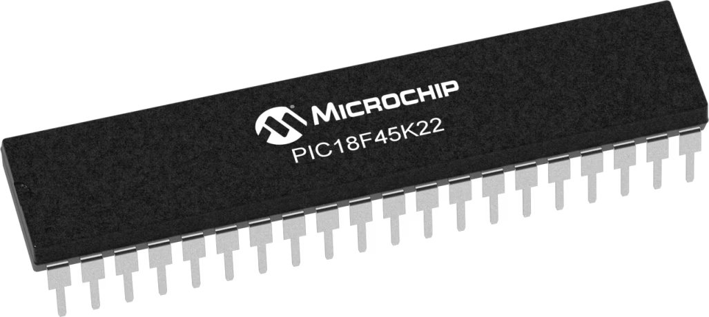
PIC18LF45K22
Our RF switch solution empowers engineers with a versatile tool for selecting and routing RF signals, enhancing system flexibility and signal quality
A
A
Hardware Overview
How does it work?
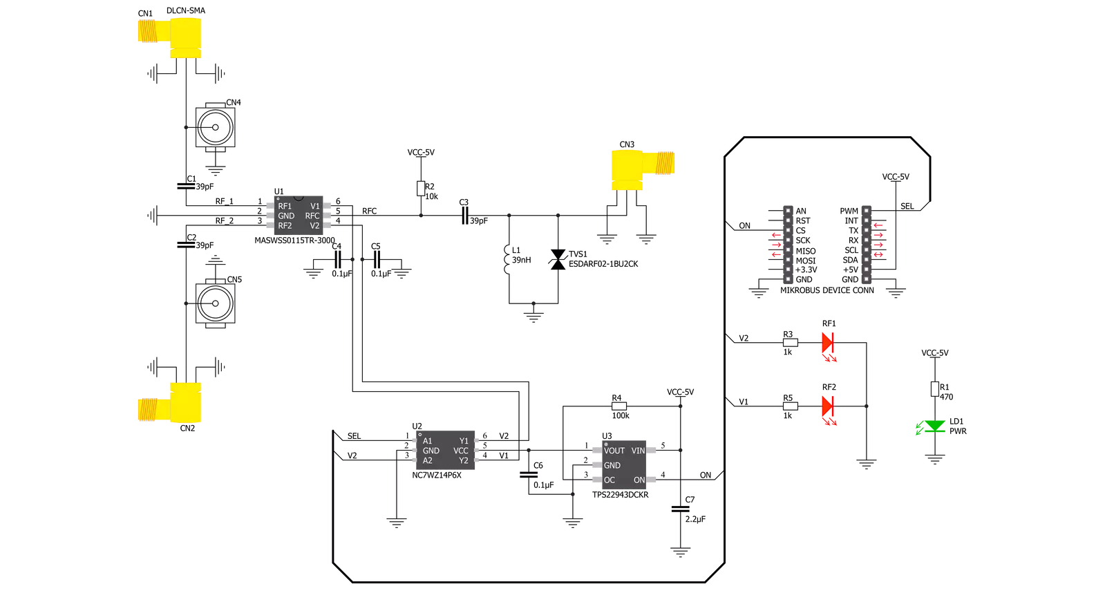
RF Switch Click is based on the MASWSS0115, a GaAs PHEMT MMIC single-pole, double-throw (SPDT) switch from Macom in a low cost, lead-free SC-70 (SOT-363) surface mount plastic package. The MASWSS0115 is ideally suited for applications where a very small size and low cost are required. Typical applications are dual-band systems that require switching between small signal components such as filter banks, single-band LNAs, converters, etc. This part can be used for low power, low loss requirements in all systems operating up to 3 GHz, including PCS, GSM, DCS, Bluetooth, and other receive chain applications.
The MASWSS0115 is fabricated using a 0.5 micron gate length GaAs PHEMT process. The process features full passivation for performance and reliability. Featured chip MASWSS0115 provides signal switching of 50MHz to up to 3GHz with an insertion loss of 0.3 dB at 2.4 GHz and power consumption of 5 µA at +2.3V. Ultra High-Speed CMOS inverter labeled as NC7WZ14 is used for driving and controlling an RF switch with the typical switching time of 3,2 ns. Additionally, a load switch TPS22943 can enable or disable the RF switch by electrically detaching the power supply. RF Switch click uses the 5V to supply the
switch driver while 3.3V microcontroller can be used to communicate with the control circuitry. Two LEDs (RF1 and RF2) indicate the current active RF port as a visual representation of a state of the switch. Since RF1 is complementary to RF2, the switching can be achieved with only one GPIO pin. The RFC is an input of the switch with the possibility of redirecting the RF signal to RF1 or RF2 port. Besides switching SEL pin, the pin labeled as ON is used for power control. All of the switch ports are accessible on the connectors located on top of the click board with the addition of miniature coaxial connectors for both RF ports.


Features overview
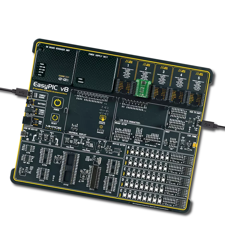
Development board
EasyPIC v7a is the seventh generation of PIC development boards specially designed for the needs of rapid development of embedded applications. It supports a wide range of 8-bit PIC microcontrollers from Microchip and has a broad set of unique functions, such as the first-ever embedded debugger/programmer over USB-C. The development board is well organized and designed so that the end-user has all the necessary elements in one place, such as switches, buttons, indicators, connectors, and others. With four different connectors for each port, EasyPIC v7a allows you to connect accessory boards, sensors, and custom electronics more efficiently than ever. Each part of the EasyPIC v7a development board
contains the components necessary for the most efficient operation of the same board. In addition to the advanced integrated CODEGRIP programmer/debugger module, which offers many valuable programming/debugging options and seamless integration with the Mikroe software environment, the board also includes a clean and regulated power supply module for the development board. It can use various external power sources, including an external 12V power supply, 7-23V AC or 9-32V DC via DC connector/screw terminals, and a power source via the USB Type-C (USB-C) connector. Communication options such as USB-UART and RS-232 are also included, alongside the well-
established mikroBUS™ standard, three display options (7-segment, graphical, and character-based LCD), and several different DIP sockets. These sockets cover a wide range of 8-bit PIC MCUs, from PIC10F, PIC12F, PIC16F, PIC16Enh, PIC18F, PIC18FJ, and PIC18FK families. EasyPIC v7a is an integral part of the Mikroe ecosystem for rapid development. Natively supported by Mikroe software tools, it covers many aspects of prototyping and development thanks to a considerable number of different Click boards™ (over a thousand boards), the number of which is growing every day.

Microcontroller Overview
MCU Card / MCU
Architecture
PIC
MCU Memory (KB)
32
Silicon Vendor
Microchip
Pin count
40
RAM (Bytes)
1536
Used MCU Pins
mikroBUS™ mapper
Take a closer look
Click board™ Schematic
Step by step
Project assembly

Start by selecting your development board and Click board™. Begin with the EasyPIC v7a as your development board.


Track your results in real time
Application Output
1. Application Output - In Debug mode, the 'Application Output' window enables real-time data monitoring, offering direct insight into execution results. Ensure proper data display by configuring the environment correctly using the provided tutorial.

2. UART Terminal - Use the UART Terminal to monitor data transmission via a USB to UART converter, allowing direct communication between the Click board™ and your development system. Configure the baud rate and other serial settings according to your project's requirements to ensure proper functionality. For step-by-step setup instructions, refer to the provided tutorial.

3. Plot Output - The Plot feature offers a powerful way to visualize real-time sensor data, enabling trend analysis, debugging, and comparison of multiple data points. To set it up correctly, follow the provided tutorial, which includes a step-by-step example of using the Plot feature to display Click board™ readings. To use the Plot feature in your code, use the function: plot(*insert_graph_name*, variable_name);. This is a general format, and it is up to the user to replace 'insert_graph_name' with the actual graph name and 'variable_name' with the parameter to be displayed.

Software Support
Library Description
This library contains API for RF Switch Click driver.
Key functions:
rfswitch_power_on- RF Switch power on functionrfswitch_switch_channel- RF Switch switch channel functionrfswitch_select_channel- RF Switch select channel function.
Open Source
Code example
The complete application code and a ready-to-use project are available through the NECTO Studio Package Manager for direct installation in the NECTO Studio. The application code can also be found on the MIKROE GitHub account.
/*!
 * @file main.c
 * @brief RF Switch Click Example.
 *
 * # Description
 * This is an example that demonstrates the use of the RF Switch Click board.
 *
 * The demo application is composed of two sections :
 *
 * ## Application Init
 * Initialization driver enable's - GPIO, also write log and powers on device.
 *
 * ## Application Task
 * Waiting for valid user input and executes functions based on set of valid commands.
 * Results are being sent to the Usart Terminal where you can track their changes.
 *
 * @author Stefan Ilic
 *
 */

#include "board.h"
#include "log.h"
#include "rfswitch.h"

static rfswitch_t rfswitch;   /**< RF Switch Click driver object. */
static log_t logger;    /**< Logger object. */

void application_init ( void )
{
    log_cfg_t log_cfg;  /**< Logger config object. */
    rfswitch_cfg_t rfswitch_cfg;  /**< Click config object. */

    /**
     * Logger initialization.
     * Default baud rate: 115200
     * Default log level: LOG_LEVEL_DEBUG
     * @note If USB_UART_RX and USB_UART_TX
     * are defined as HAL_PIN_NC, you will
     * need to define them manually for log to work.
     * See @b LOG_MAP_USB_UART macro definition for detailed explanation.
     */
    LOG_MAP_USB_UART( log_cfg );
    log_init( &logger, &log_cfg );
    log_info( &logger, " Application Init " );

    // Click initialization.
    rfswitch_cfg_setup( &rfswitch_cfg );
    RFSWITCH_MAP_MIKROBUS( rfswitch_cfg, MIKROBUS_1 );
    if ( DIGITAL_OUT_UNSUPPORTED_PIN == rfswitch_init( &rfswitch, &rfswitch_cfg ) )
    {
        log_error( &logger, " Communication init." );
        for ( ; ; );
    }
    log_printf( &logger, "------------------------\r\n" );
    log_printf( &logger, "   Powering device on   \r\n" );
    rfswitch_power_on( &rfswitch );
    Delay_ms ( 100 );
    log_printf( &logger, "------------------------\r\n" );
    log_printf( &logger, "   Select option to     \r\n" );
    log_printf( &logger, "    select channel      \r\n" );
    log_printf( &logger, "------------------------\r\n" );
    log_printf( &logger, " 1. Channel 1 selected  \r\n" );
    log_printf( &logger, " 2. Channel 2 selected  \r\n" );
    log_printf( &logger, " 3. Switching channel   \r\n" );
    log_printf( &logger, "------------------------\r\n" );
}

void application_task ( void )
{
    uint8_t tx_buf;
    if ( log_read( &logger, &tx_buf, 1 ) ) {
        switch ( tx_buf ) {
            case '1' : {
                rfswitch_select_channel( &rfswitch, RFSWITCH_SELECT_CHANNEL_1 );
                log_printf( &logger, " Switching to RF port 1 \r\n" );
                log_printf( &logger, "------------------------\r\n" );
                break;
            }
            case '2' : {
                rfswitch_select_channel( &rfswitch, RFSWITCH_SELECT_CHANNEL_2 );
                log_printf( &logger, " Switching to RF port 2 \r\n" );
                log_printf( &logger, "------------------------\r\n" );
                break;
            }
            case '3' : {
                rfswitch_switch_channel( &rfswitch );
                log_printf( &logger, "   Switching RF port    \r\n" );
                log_printf( &logger, "------------------------\r\n" );
                break;
            }
            default : {
                log_printf( &logger, "   Select option to     \r\n" );
                log_printf( &logger, "    select channel      \r\n" );
                log_printf( &logger, "------------------------\r\n" );
                log_printf( &logger, " 1. Channel 1 selected  \r\n" );
                log_printf( &logger, " 2. Channel 2 selected  \r\n" );
                log_printf( &logger, " 3. Switching channel   \r\n" );
                log_printf( &logger, "------------------------\r\n" );
            }
        }
    }
}

int main ( void )
{
    /* Do not remove this line or clock might not be set correctly. */
    #ifdef PREINIT_SUPPORTED
    preinit();
    #endif

    application_init( );

    for ( ; ; )
    {
        application_task( );
    }

    return 0;
}

// ------------------------------------------------------------------------ END
Additional Support
Resources
Category:Port expander