Experience flawless analog-to-digital conversion with AD7124-8 and ATmega644P
Capturing the analog world, shaping the digital future

Published Jun 08, 2023
Click board™
ADC 6 Click
Dev. board
EasyAVR v7
Compiler
NECTO Studio
MCU
ATmega644P
Take your engineering solutions to the next level with our state-of-the-art ADC
A
A
Hardware Overview
How does it work?
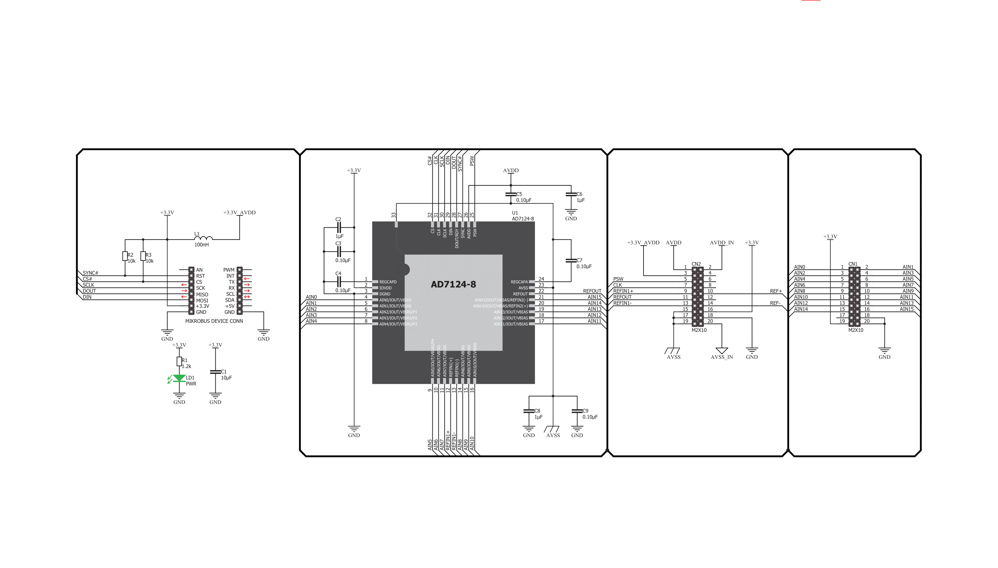
ADC 6 Click is based on the AD7124-8, an 8-channel, low noise, low power, 24bit sigma-delta ADC with reference and programmable gain array from Analog Devices. This IC offers several different power modes and input connection configurations, giving much flexibility to work with. The device can have eight differential or 15 pseudo-differential analog inputs and any combination between them. All the input channels can be configured to be either buffered or unbuffered, depending on the input connection impedance characteristics. The maximum output data rate varies from 2400SPS to 19,200SPS (samples per second) concerning the selected power mode. An ultra-low noise operation produces 22 noise-free bits in all available power modes. The signal routing in the AD7124-8 ADC is done via the internal multiplexer section, which reduces the number of IC pins, yet allows all of the functions to be used on the existing pins. On top of these pins, four more GPIO pins can be used for various tasks, including control of the multiplexer unit. Since the multiplexer is integrated into the chip, the conversion process stays synchronized with the changes made to the pin configuration. So-called setups further manage the input signal. There are eight such setups available on the AD7124-8 ADC module. A single setup consists of four different registers: configuration register, filter register, gain register, an offset register. These registers configure the corresponding set of functions for the connected channel(s). The channel
register is used to configure the basic settings for the corresponding ADC channel, among other options, which of the eight available setups to connect with that channel. This mechanism allows easy configuration of multiple channels, especially when the same settings must be applied to more than one channel, greatly reducing the software complexity since the setups can be reused. An internal bias voltage generator can be routed to the output pins. It is used to bias the negative terminal of the selected input channel. This function is useful in thermocouple applications, as the voltage generated by the thermocouple must be biased around some DC voltage when the ADC operates from a single power supply. The AD7124-8 ADC module is clocked by either an internal clock source, which works at 614.4 kHz. The CLK pin can be used either to output the clock signal available on the ADC or to use the external clock input. This allows the synchronizing of several devices by using the same clock frequency. The internal clock speed is divided depending on the selected operating mode. Selecting low-power operating modes will impact the samples per second that this device can perform. ADC 6 Click uses the SPI interface for communication with the host MCU. The SPI bus pins are routed to the mikroBUS™ SPI pins (MISO, MOSI, SCK, and CS), allowing easy integration with the development system. The device uses SPI mode 3, which means that the clock signal (SCK) is idle HIGH, and the
rising edge of SCLK is the sample edge. The data is clocked out on the falling edge and clocked in on the rising edge of the clock signal pulse. The Data Out pin of the ADC module (DOUT/#RDY) is routed to the mikroBUS™ MISO pin, and besides for the data output, is also used to signal the presence of the valid data in the ADC output shift register. When a valid reading is stored in this register, the #RDY signal will be pulled to a LOW state, indicating the ready status of the data output register. It can be used to trigger an interrupt on the host MCU. The #SYNC pin of the ADC module is used to synchronize reading when more than one device is used. While pulled to a LOW state, the internal ADC sections are reset and held in the reset state. This pin is pulled to a HIGH logic level via the onboard resistor. This pin is routed to the mikroBUS™ RST pin. Several pins are routed to the 2x10 standard pitch of 2.54mm (100mils) header. This allows even easier routing with jumpers or jumper wires, as the header can further configure the ADC in a way impossible by software, i.e., connecting an external clock source or reference voltages. The complete layout of this header can be seen on the schematics of the ADC 6 click. The second 2x10 header is used to connect the input signals. The AD7124-8 ADC module allows several kinds of signals to be routed to these pins via the multiplexing section, allowing diagnostic functions to be interleaved with the conversion of the analog signals.

Features overview
Development board
EasyAVR v7 is the seventh generation of AVR development boards specially designed for the needs of rapid development of embedded applications. It supports a wide range of 16-bit AVR microcontrollers from Microchip and has a broad set of unique functions, such as a powerful onboard mikroProg programmer and In-Circuit debugger over USB. The development board is well organized and designed so that the end-user has all the necessary elements in one place, such as switches, buttons, indicators, connectors, and others. With four different connectors for each port, EasyAVR v7 allows you to connect accessory boards, sensors, and custom electronics more
efficiently than ever. Each part of the EasyAVR v7 development board contains the components necessary for the most efficient operation of the same board. An integrated mikroProg, a fast USB 2.0 programmer with mikroICD hardware In-Circuit Debugger, offers many valuable programming/debugging options and seamless integration with the Mikroe software environment. Besides it also includes a clean and regulated power supply block for the development board. It can use a wide range of external power sources, including an external 12V power supply, 7-12V AC or 9-15V DC via DC connector/screw terminals, and a power source via the USB Type-B (USB-B)
connector. Communication options such as USB-UART and RS-232 are also included, alongside the well-established mikroBUS™ standard, three display options (7-segment, graphical, and character-based LCD), and several different DIP sockets which cover a wide range of 16-bit AVR MCUs. EasyAVR v7 is an integral part of the Mikroe ecosystem for rapid development. Natively supported by Mikroe software tools, it covers many aspects of prototyping and development thanks to a considerable number of different Click boards™ (over a thousand boards), the number of which is growing every day.

Microcontroller Overview
MCU Card / MCU
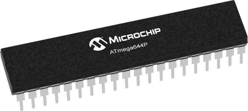
Architecture
AVR
MCU Memory (KB)
64
Silicon Vendor
Microchip
Pin count
40
RAM (Bytes)
4096
Used MCU Pins
mikroBUS™ mapper
Take a closer look
Click board™ Schematic
Step by step
Project assembly

Start by selecting your development board and Click board™. Begin with the EasyAVR v7 as your development board.


Software Support
Library Description
This library contains API for ADC 6 Click driver.
Key functions:
adc6_get_adc_dataGet data functionadc6_read_regGeneric read functionadc6_write_regGeneric write function
Open Source
Code example
The complete application code and a ready-to-use project are available through the NECTO Studio Package Manager for direct installation in the NECTO Studio. The application code can also be found on the MIKROE GitHub account.
/*!
 * \file
 * \brief ADC6 Click example
 *
 * # Description
 * This application collects data from the sensor, calculates the voltage to a
 * digital value and then logs it.
 *
 * The demo application is composed of two sections :
 *
 * ## Application Init
 * Initializes driver and sets configuration which enables channel 0,
 * puts AIN0 on positive analog input and AIN1 on negative analog input,
 * enables internal reference voltage (approximately 2.65V (AVDD = 3.3V)),
 * and also enables bipolar operation mode and puts device on full power mode.
 * When the ADC is configured for unipolar operation, the output code is natural
 * (straight) binary with a zero differential input voltage
 * resulting in a code of 0x00000000, a midscale voltage resulting in a code
 * of 0x00800000, and a full-scale input voltage resulting in a code of 0x00FFFFFF.
 * When the ADC is configured for bipolar operation, the output code is offset
 * binary with a negative full-scale voltage resulting in a code of 0x00000000,
 * a zero differential input voltage resulting in a code of 0x00800000,
 * and a positive full-scale input voltage resulting in a code of 0x00FFFFFF.
 *
 * ## Application Task
 * Gets 24-bit converted data in single read mode and logs data on USB UART.
 * Repeats operation every 500 ms.
 *
 *
 * \author MikroE Team
 *
 */
// ------------------------------------------------------------------- INCLUDES

#include "board.h"
#include "log.h"
#include "adc6.h"

// ------------------------------------------------------------------ VARIABLES

static adc6_t adc6;
static log_t logger;

// ------------------------------------------------------ APPLICATION FUNCTIONS

void application_init ( void )
{
    log_cfg_t log_cfg;
    adc6_cfg_t cfg;

    /**
     * Logger initialization.
     * Default baud rate: 115200
     * Default log level: LOG_LEVEL_DEBUG
     * @note If USB_UART_RX and USB_UART_TX
     * are defined as HAL_PIN_NC, you will
     * need to define them manually for log to work.
     * See @b LOG_MAP_USB_UART macro definition for detailed explanation.
     */
    LOG_MAP_USB_UART( log_cfg );
    log_init( &logger, &log_cfg );
    log_info( &logger, "---- Application Init ----" );

    //  Click initialization.

    adc6_cfg_setup( &cfg );
    ADC6_MAP_MIKROBUS( cfg, MIKROBUS_1 );
    adc6_init( &adc6, &cfg );
    adc6_default_cfg( &adc6 );
}

void application_task ( void )
{
    uint32_t adc_value = 0;

    adc_value = adc6_get_adc_data( &adc6 );

    log_printf( &logger, "The ADC value is: 0x%.6LX\r\n", adc_value );

    Delay_ms ( 500 );
}

int main ( void )
{
    /* Do not remove this line or clock might not be set correctly. */
    #ifdef PREINIT_SUPPORTED
    preinit();
    #endif

    application_init( );

    for ( ; ; )
    {
        application_task( );
    }

    return 0;
}

// ------------------------------------------------------------------------ END


