Achieve crystal-clear analog-to-digital conversion with ADS1115 and MK22FN512VLH12
Empowering data transformation

Published Jun 08, 2023
Click board™
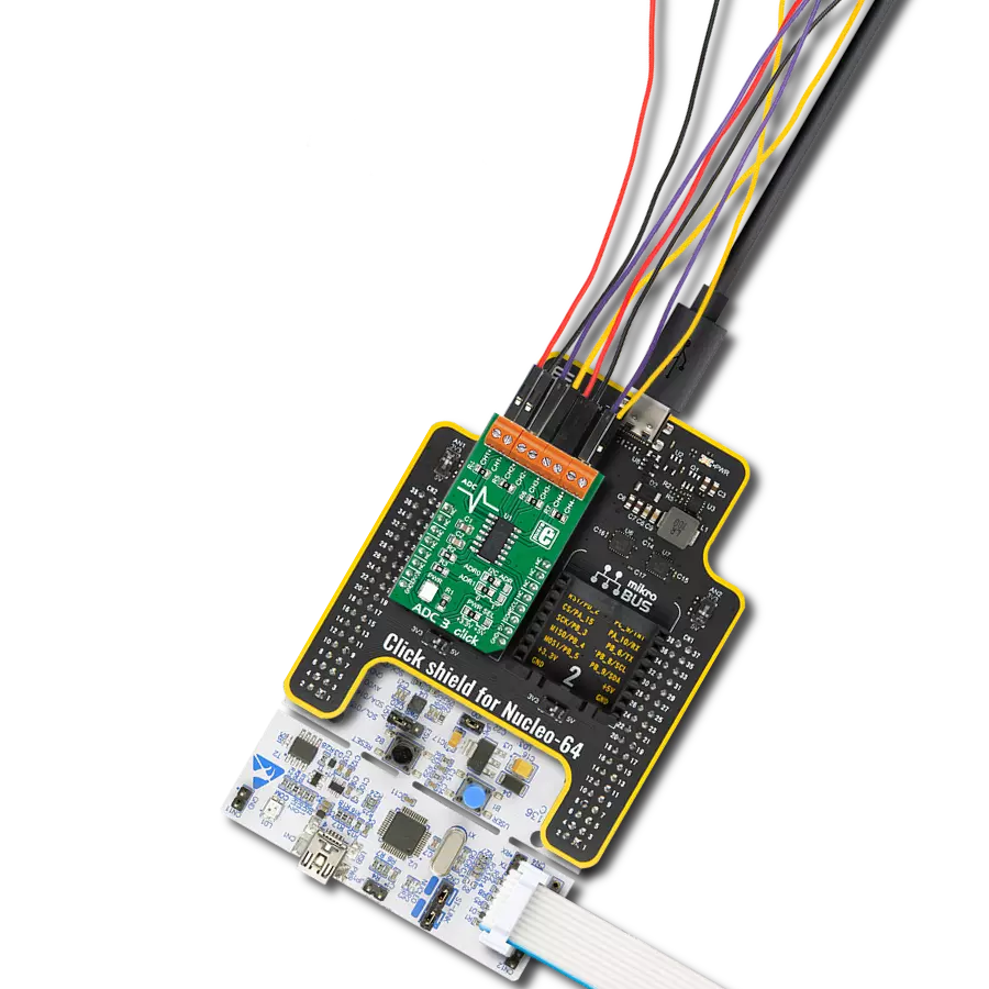
ADC 8 Click
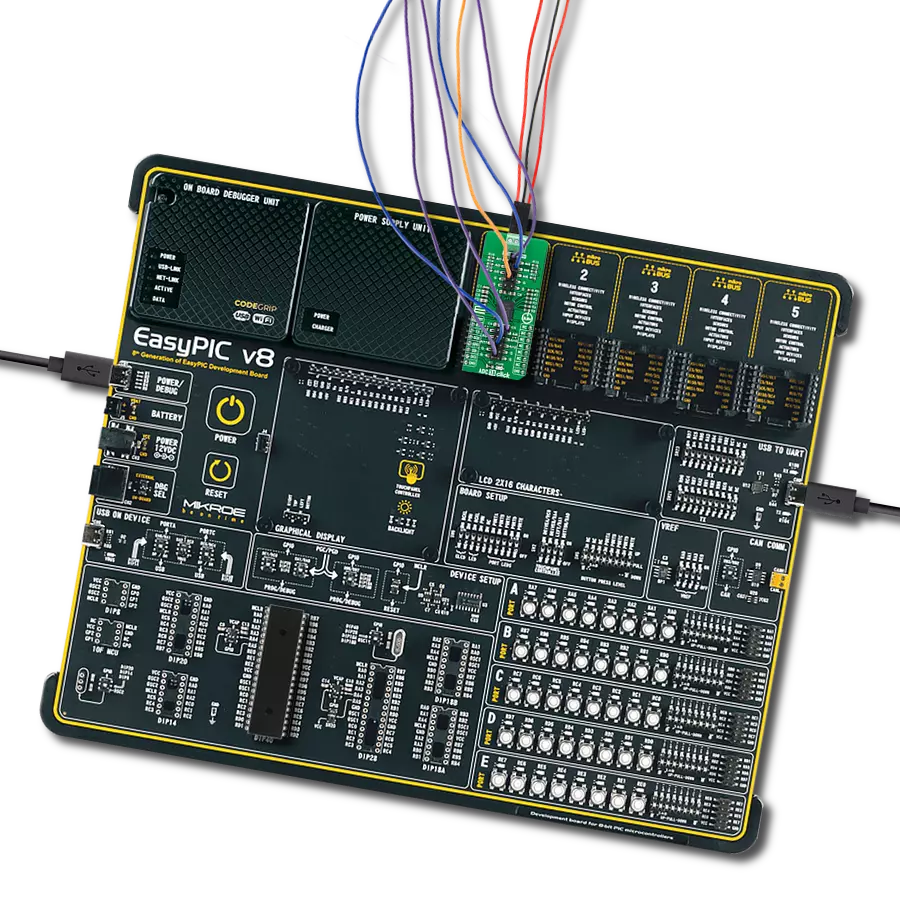
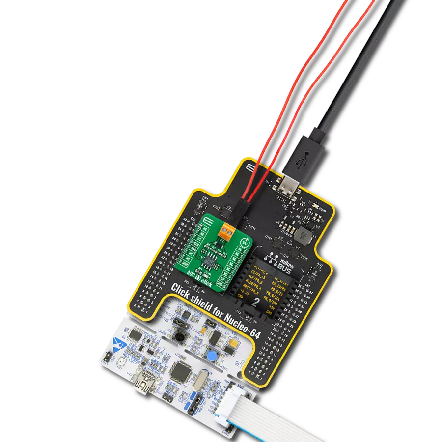
Dev. board
Kinetis Clicker
Compiler
NECTO Studio
MCU
MK22FN512VLH12
Ready to take your designs to new heights? Discover how our ADC solution can elevate your design!
A
A
Hardware Overview
How does it work?
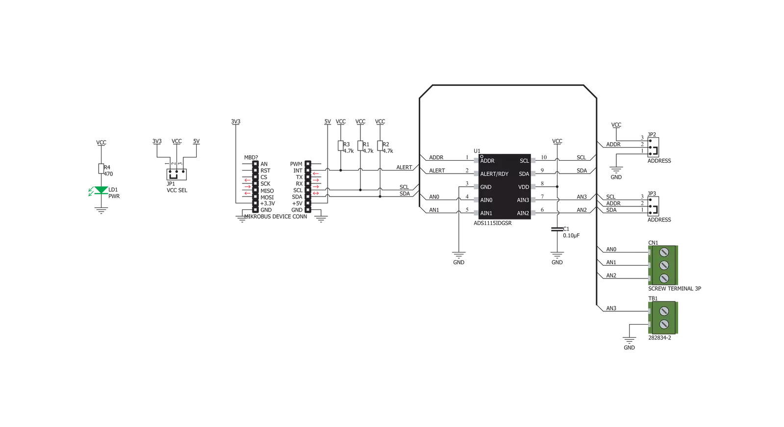
ADC 8 Click is based on the ADS1115, an ultra-small, low-power, high-precision, 16-bit A/D converter from Texas Instruments. It is a delta-sigma converter with an integrated high-precision voltage reference, which can be programmed in several different steps. The maximum data rate of this ADC is 860 SPS; however, it features an excellent signal-to-noise ratio (SNR). The ADS1115 has two differential or four single-ended inputs. The internal multiplexer is used to select the active input. The input pins are routed to two input terminals on the edge of the Click board™, allowing it to be easily interfaced with the analog signal source. Besides the power supply and I2C interface pins, the ADS1115 has an additional ALERT/RDY pin to signal conversion data available on the output register. This pin can also be set to output an overvoltage event. An internal comparator module can detect if the
input signal exceeds the voltage reference level and report the overvoltage event at the ALERT/RDY pin. This pin is routed to the mikroBUS™ INT pin. Both I2C pins, along with the ALERT/RDY pin, are pulled to a HIGH logic level by the pull-up resistors. The conversion output is available over the I2C interface in 16-bit two’s complement LSB/MSB format. A positive input signal can have values from 0x0001 to 0x7FFF, while the negative input signal can have values from 0x0000 to 0x8000. The slave I2C address of the device can be selected by moving the SMD jumper labeled as ADDR. It allows four different I2C addresses to be selected, and thus, up to four different ADC 8 clicks can be used on a single I2C bus. The signal to Noise ratio (SNR) depends on the reference voltage and output data rate. Delta-sigma ADCs are based on the oversampling principle: the input signal is sampled at a
higher frequency and filtered and decimated until the output value is obtained at the requested output data rate. The ratio between the high sampling frequency (modulator) and the output data rate is called oversampling ratio (OSR). Increasing the OSR, less noise appears at the output since more values are included in the averaging process. As mentioned, the ADS1115 IC cannot use an external voltage reference. However, it has a high-precision internal reference with low drift over temperature. It can be selected from several available values: ±0.256, ±0.512, ±1.024, ±2.048V, ±4.096, and ±6.144. Note, however, that the input signal should not be greater than VCC + 0.3V. In other words, it is not possible to use the 4.096V if the power supply source is 3.3V. ADC 8 click is equipped with the SMD jumper labeled as VCC SEL, which allows selection between 3.3V and 5V.

Features overview
Development board
Kinetis Clicker is a compact starter development board that brings the flexibility of add-on Click boards™ to your favorite microcontroller, making it a perfect starter kit for implementing your ideas. It comes with an onboard 32-bit ARM Cortex-M4 microcontroller, the MK22FN512VLH12 from NXP Semiconductor, a USB connector, LED indicators, buttons, a mikroProg connector, and a header for interfacing with external electronics. Thanks to its compact design with clear and easy-recognizable silkscreen markings, it provides a fluid and immersive working experience, allowing access
anywhere and under any circumstances. Each part of the Kinetis Clicker development kit contains the components necessary for the most efficient operation of the same board. In addition to the possibility of choosing the Kinetis Clicker programming method, using USB HID mikroBootloader, or through an external mikroProg connector for Kinetis programmer, the Clicker board also includes a clean and regulated power supply module for the development kit. The USB-MiniAB connection provides up to 500mA of current, which is more than enough to operate all
onboard and additional modules. All communication methods that mikroBUS™ itself supports are on this board, including the well-established mikroBUS™ socket, reset button, and several buttons and LED indicators. Kinetis Clicker is an integral part of the Mikroe ecosystem, allowing you to create a new application in minutes. Natively supported by Mikroe software tools, it covers many aspects of prototyping thanks to a considerable number of different Click boards™ (over a thousand boards), the number of which is growing every day.

Microcontroller Overview
MCU Card / MCU
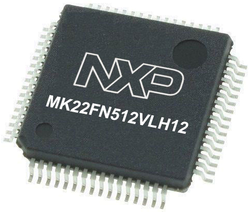
Architecture
ARM Cortex-M4
MCU Memory (KB)
512
Silicon Vendor
NXP
Pin count
64
RAM (Bytes)
131072
Used MCU Pins
mikroBUS™ mapper
Take a closer look
Click board™ Schematic
Step by step
Project assembly

Start by selecting your development board and Click board™. Begin with the Kinetis Clicker as your development board.


Track your results in real time
Application Output
1. Application Output - In Debug mode, the 'Application Output' window enables real-time data monitoring, offering direct insight into execution results. Ensure proper data display by configuring the environment correctly using the provided tutorial.

2. UART Terminal - Use the UART Terminal to monitor data transmission via a USB to UART converter, allowing direct communication between the Click board™ and your development system. Configure the baud rate and other serial settings according to your project's requirements to ensure proper functionality. For step-by-step setup instructions, refer to the provided tutorial.

3. Plot Output - The Plot feature offers a powerful way to visualize real-time sensor data, enabling trend analysis, debugging, and comparison of multiple data points. To set it up correctly, follow the provided tutorial, which includes a step-by-step example of using the Plot feature to display Click board™ readings. To use the Plot feature in your code, use the function: plot(*insert_graph_name*, variable_name);. This is a general format, and it is up to the user to replace 'insert_graph_name' with the actual graph name and 'variable_name' with the parameter to be displayed.

Software Support
Library Description
This library contains API for ADC 8 Click driver.
Key functions:
adc8_get_diff_channel- Get diff channel voltageadc8_get_single_channel- Get single channel voltageadc8_get_interrupt_state- Get interrupt pin state
Open Source
Code example
The complete application code and a ready-to-use project are available through the NECTO Studio Package Manager for direct installation in the NECTO Studio. The application code can also be found on the MIKROE GitHub account.
/*!
 * \file
 * \brief Adc8 Click example
 *
 * # Description
 * The demo app shows voltage measurement across all singles and different channels.
 *
 * The demo application is composed of two sections :
 *
 * ## Application Init
 * Configuring Clicks and log objects.
 * Settings the Click in the default configuration.
 *
 * ## Application Task
 * Reads voltage from each channel one by one and the voltage difference
 * between specified channels.
 *
 * *note:*
 * On the input channel AIN0, AIN1, AIN2 and AIN3 sets maximum voltage
 * GND - 0.3V < VIN > VDD + 0.3V
 *
 * \author Katarina Perendic
 *
 */
// ------------------------------------------------------------------- INCLUDES

#include "board.h"
#include "log.h"
#include "adc8.h"

// ------------------------------------------------------------------ VARIABLES

static adc8_t adc8;
static log_t logger;

// ------------------------------------------------------ APPLICATION FUNCTIONS

void application_init ( void )
{
    log_cfg_t log_cfg;
    adc8_cfg_t cfg;

    /**
     * Logger initialization.
     * Default baud rate: 115200
     * Default log level: LOG_LEVEL_DEBUG
     * @note If USB_UART_RX and USB_UART_TX
     * are defined as HAL_PIN_NC, you will
     * need to define them manually for log to work.
     * See @b LOG_MAP_USB_UART macro definition for detailed explanation.
     */
    LOG_MAP_USB_UART( log_cfg );
    log_init( &logger, &log_cfg );
    log_info( &logger, "---- Application Init ----" );

    //  Click initialization.

    adc8_cfg_setup( &cfg );
    ADC8_MAP_MIKROBUS( cfg, MIKROBUS_1 );
    adc8_init( &adc8, &cfg );

    adc8_default_cfg( &adc8 );
    log_info( &logger, "---- ADC start ----" );
}

void application_task ( void )
{
    adc8_single_volt_t single_volt;
    adc8_diff_volt_t diff_volt;

    log_printf( &logger, "\r\n-----------------------------------" );

    // Single channel
    adc8_get_single_channel( &adc8, &single_volt );

    log_printf( &logger, "\r\n>>> SINGLE CHANNEL <<<<\r\n" );
    log_printf( &logger, "- CH 0: %.2f\r\n", single_volt.ch_0 );
    log_printf( &logger, "- CH 1: %.2f\r\n", single_volt.ch_1 );
    log_printf( &logger, "- CH 2: %.2f\r\n", single_volt.ch_2 );
    log_printf( &logger, "- CH 3: %.2f\r\n", single_volt.ch_3 );

    // Diff channel

    adc8_get_diff_channel( &adc8, &diff_volt );

    log_printf( &logger, "\r\n>>> DIFF CHANNEL <<<<\r\n" );
    log_printf( &logger, "- CH(0-1): %.2f\r\n", diff_volt.ch_0_1 );
    log_printf( &logger, "- CH(0-3): %.2f\r\n", diff_volt.ch_0_3 );
    log_printf( &logger, "- CH(1-3): %.2f\r\n", diff_volt.ch_1_3 );
    log_printf( &logger, "- CH(2-3): %.2f\r\n", diff_volt.ch_2_3 );

    Delay_ms ( 1000 );
}

int main ( void )
{
    /* Do not remove this line or clock might not be set correctly. */
    #ifdef PREINIT_SUPPORTED
    preinit();
    #endif

    application_init( );

    for ( ; ; )
    {
        application_task( );
    }

    return 0;
}


// ------------------------------------------------------------------------ END