Control both inductive and resistive loads in environments such as industrial settings using TPD2017FN and MK22FN512VLH12
Low-side switch (8-channels) for motors, solenoids, lamp drives

Published Mar 01, 2024
Click board™
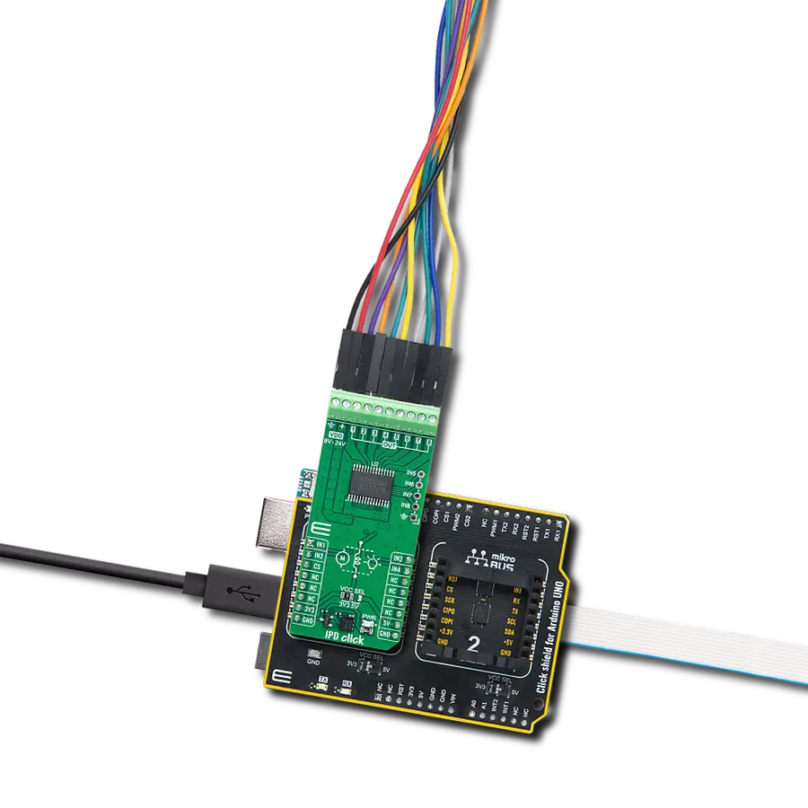
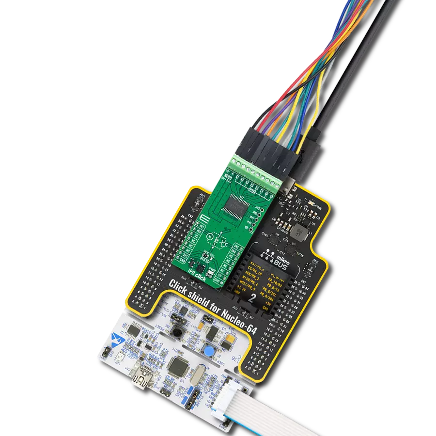
IPD Click -2017
Dev. board
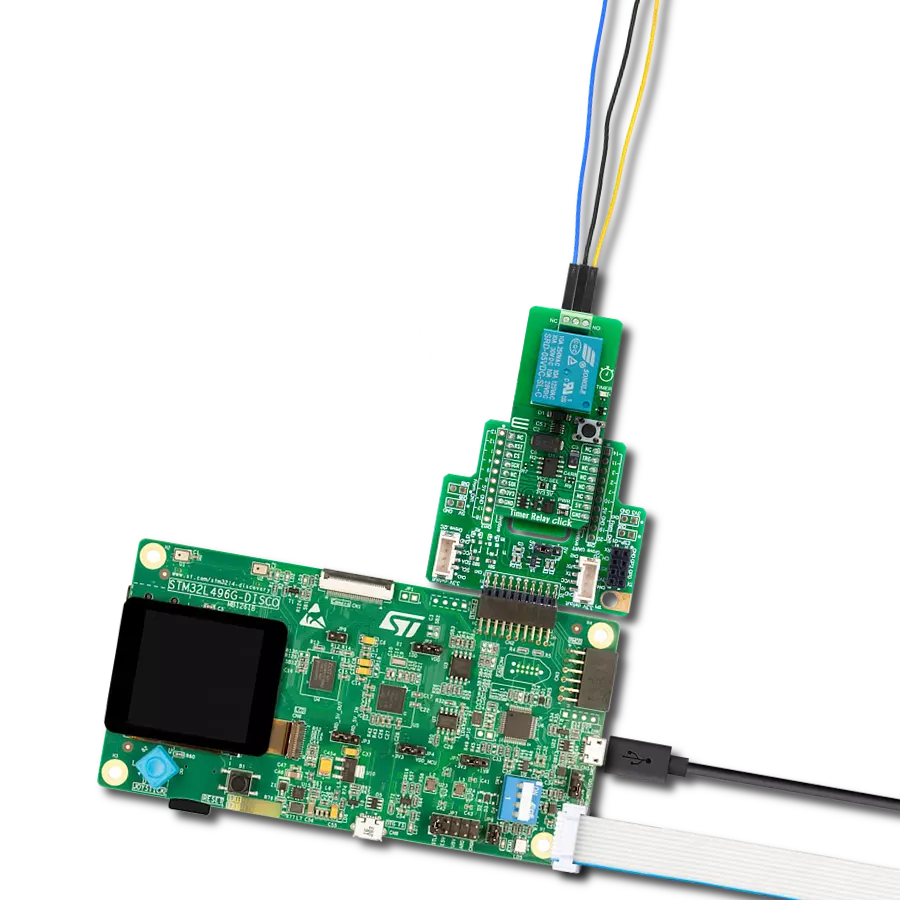
Kinetis Clicker
Compiler
NECTO Studio
MCU
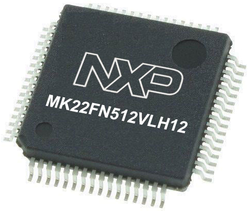
MK22FN512VLH12
Enhance automation in industrial environments and applications that need managing resistive and inductive loads up to 50mH, featuring a current capability of 0.5A for each channel
A
A
Hardware Overview
How does it work?
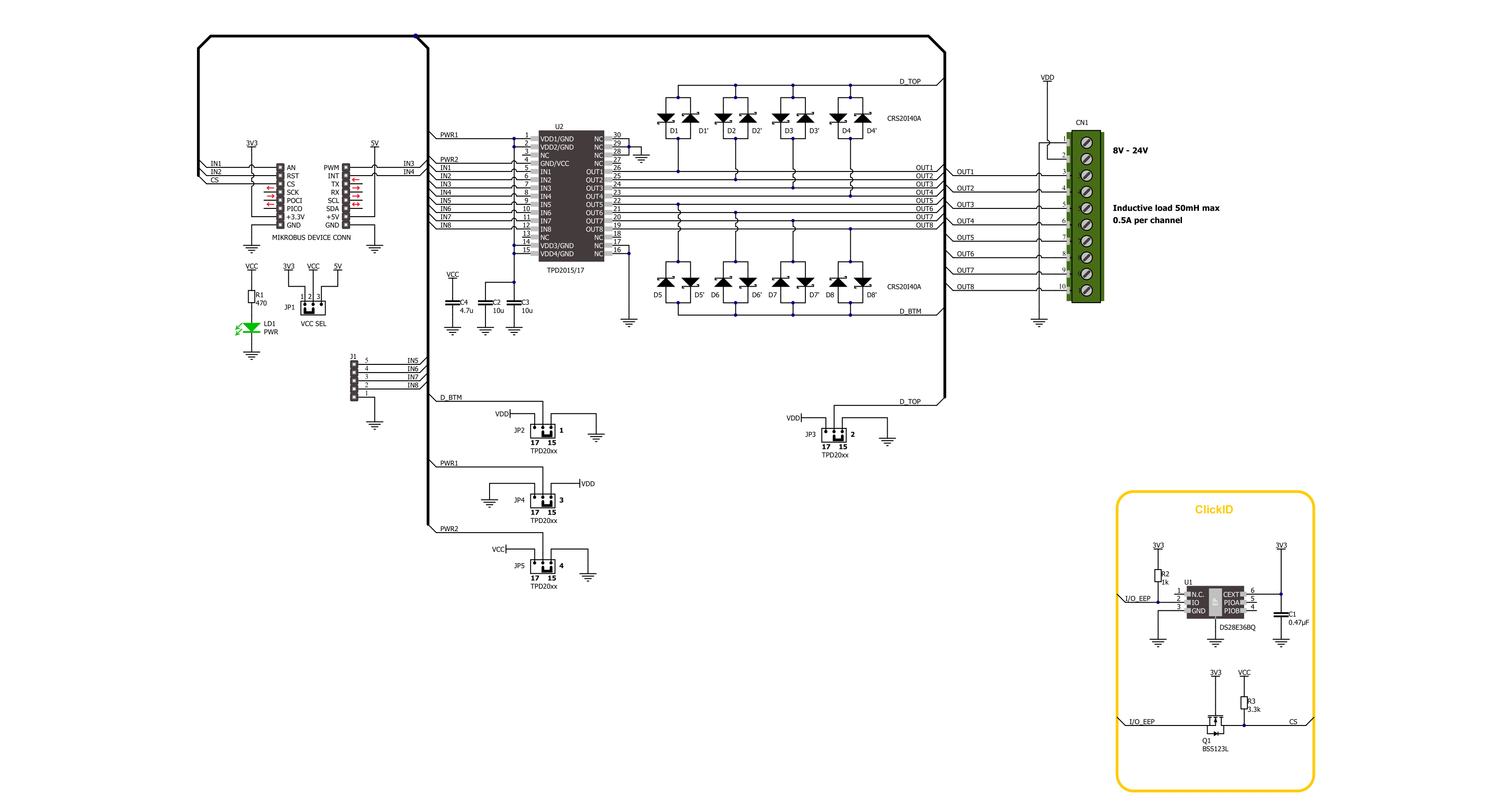
IPD Click - 2017 is based on the TPD2017FN, an 8-channel low-side switch featuring MOSFET outputs from Toshiba Semiconductor, designed to be directly driven by CMOS and TTL logic circuitry. It's ideally suited for driving inductive and resistive loads, such as industrial programmable logic controllers for industrial use, motors, relays, lamps in factory automation equipment, and more. A key advantage of the TPD2017FN is its built-in overcurrent and overtemperature protection, enhancing system stability by safeguarding against excessive heat and current. Equipped with the capability to handle back electromotive force from inductive loads without surpassing the component's voltage tolerance, the TPD2017FN is optimized for loads up to 50mH with a current capacity of 0.5A per channel, supported by an external power supply ranging from 8-24V. The channels can be
operated in parallel to increase the current capability of the outputs. As mentioned, this Click board™ incorporates comprehensive protection mechanisms, including overtemperature protection that deactivates all outputs (OUT1-OUT8) if the temperature exceeds 175°C and overcurrent protection that limits voltage and current during load shorts, ensuring the device and its connected peripheral safety. Designed for straightforward integration with CMOS and TTL systems, the IPD Click features input control terminals for each output channel, allowing independent channel control. Inputs IN1 to IN4 interface directly via the mikroBUS™ socket, with additional inputs IN5 to IN8 accessible through an unpopulated header. Each input control pin of the TPD2017FN is equipped with a built-in 300kΩ pull-down resistor to maintain a LOW logic state in an open state. This
Click board™ comes with optional inductive load decoupling diodes unpopulated by default, the CRS20140A from Toshiba Semiconductor, allowing users to add them in the case of higher inductive loads. Also, it is equipped with jumpers for the diode configuration of the used load switch and its power management. These jumpers are pre-configured, enabling immediate use without the need for any adjustments. This Click board™ can operate with either 3.3V or 5V logic voltage levels selected via the VCC SEL jumper. This way, both 3.3V and 5V capable MCUs can use the communication lines properly. Also, this Click board™ comes equipped with a library containing easy-to-use functions and an example code that can be used as a reference for further development.

Features overview
Development board
Kinetis Clicker is a compact starter development board that brings the flexibility of add-on Click boards™ to your favorite microcontroller, making it a perfect starter kit for implementing your ideas. It comes with an onboard 32-bit ARM Cortex-M4 microcontroller, the MK22FN512VLH12 from NXP Semiconductor, a USB connector, LED indicators, buttons, a mikroProg connector, and a header for interfacing with external electronics. Thanks to its compact design with clear and easy-recognizable silkscreen markings, it provides a fluid and immersive working experience, allowing access
anywhere and under any circumstances. Each part of the Kinetis Clicker development kit contains the components necessary for the most efficient operation of the same board. In addition to the possibility of choosing the Kinetis Clicker programming method, using USB HID mikroBootloader, or through an external mikroProg connector for Kinetis programmer, the Clicker board also includes a clean and regulated power supply module for the development kit. The USB-MiniAB connection provides up to 500mA of current, which is more than enough to operate all
onboard and additional modules. All communication methods that mikroBUS™ itself supports are on this board, including the well-established mikroBUS™ socket, reset button, and several buttons and LED indicators. Kinetis Clicker is an integral part of the Mikroe ecosystem, allowing you to create a new application in minutes. Natively supported by Mikroe software tools, it covers many aspects of prototyping thanks to a considerable number of different Click boards™ (over a thousand boards), the number of which is growing every day.

Microcontroller Overview
MCU Card / MCU
Architecture
ARM Cortex-M4
MCU Memory (KB)
512
Silicon Vendor
NXP
Pin count
64
RAM (Bytes)
131072
Used MCU Pins
mikroBUS™ mapper
Take a closer look
Click board™ Schematic
Step by step
Project assembly

Start by selecting your development board and Click board™. Begin with the Kinetis Clicker as your development board.


Track your results in real time
Application Output
1. Application Output - In Debug mode, the 'Application Output' window enables real-time data monitoring, offering direct insight into execution results. Ensure proper data display by configuring the environment correctly using the provided tutorial.

2. UART Terminal - Use the UART Terminal to monitor data transmission via a USB to UART converter, allowing direct communication between the Click board™ and your development system. Configure the baud rate and other serial settings according to your project's requirements to ensure proper functionality. For step-by-step setup instructions, refer to the provided tutorial.

3. Plot Output - The Plot feature offers a powerful way to visualize real-time sensor data, enabling trend analysis, debugging, and comparison of multiple data points. To set it up correctly, follow the provided tutorial, which includes a step-by-step example of using the Plot feature to display Click board™ readings. To use the Plot feature in your code, use the function: plot(*insert_graph_name*, variable_name);. This is a general format, and it is up to the user to replace 'insert_graph_name' with the actual graph name and 'variable_name' with the parameter to be displayed.

Software Support
Library Description
This library contains API for IPD Click -2017 driver.
Key functions:
ipd2017_all_pins_set- IPD 2017 pin setting functionipd2017_set_out_level- IPD 2017 set output level functionipd2017_get_out_state- IPD 2017 get output level function
Open Source
Code example
The complete application code and a ready-to-use project are available through the NECTO Studio Package Manager for direct installation in the NECTO Studio. The application code can also be found on the MIKROE GitHub account.
/*!
 * @file main.c
 * @brief IPD 2017 Click Example.
 *
 * # Description
 * This example demonstrates the use of IPD 2017 Click board by toggling the output state.
 *
 * The demo application is composed of two sections :
 *
 * ## Application Init
 * Initializes the driver and logger.
 *
 * ## Application Task
 * Switches on all output pins state for 2 seconds, then switches them off, and turns them on one by one.
 *
 * @author Stefan Ilic
 *
 */

#include "board.h"
#include "log.h"
#include "ipd2017.h"

static ipd2017_t ipd2017;   /**< IPD 2017 Click driver object. */
static log_t logger;    /**< Logger object. */

void application_init ( void )
{
    log_cfg_t log_cfg;  /**< Logger config object. */
    ipd2017_cfg_t ipd2017_cfg;  /**< Click config object. */

    /**
     * Logger initialization.
     * Default baud rate: 115200
     * Default log level: LOG_LEVEL_DEBUG
     * @note If USB_UART_RX and USB_UART_TX
     * are defined as HAL_PIN_NC, you will
     * need to define them manually for log to work.
     * See @b LOG_MAP_USB_UART macro definition for detailed explanation.
     */
    LOG_MAP_USB_UART( log_cfg );
    log_init( &logger, &log_cfg );
    log_info( &logger, " Application Init " );

    // Click initialization.
    ipd2017_cfg_setup( &ipd2017_cfg );
    IPD2017_MAP_MIKROBUS( ipd2017_cfg, MIKROBUS_1 );
    if ( DIGITAL_OUT_UNSUPPORTED_PIN == ipd2017_init( &ipd2017, &ipd2017_cfg ) )
    {
        log_error( &logger, " Communication init." );
        for ( ; ; );
    }

    log_info( &logger, " Application Task " );
}

void application_task ( void )
{
    log_printf( &logger, " Turning OUT 1 to OUT 4 HIGH \r\n" );
    ipd2017_all_pins_set( &ipd2017 );
    Delay_ms ( 1000 );
    Delay_ms ( 1000 );

    log_printf( &logger, " Turning OUT 1 to OUT 4 LOW \r\n" );
    ipd2017_all_pins_clear( &ipd2017 );
    Delay_ms ( 1000 );
    Delay_ms ( 1000 );

    log_printf( &logger, " Turning OUT 1 to OUT 4 one by one \r\n" );
    uint8_t out_sel = IPD2017_OUT1_PIN_MASK;
    do
    {
        ipd2017_set_out_level( &ipd2017, out_sel, IPD2017_PIN_STATE_HIGH );
        Delay_ms ( 1000 );
        Delay_ms ( 1000 );
        ipd2017_set_out_level( &ipd2017, out_sel, IPD2017_PIN_STATE_LOW );
        out_sel <<=  1;
    }
    while ( out_sel <= IPD2017_OUT4_PIN_MASK );

}

int main ( void )
{
    /* Do not remove this line or clock might not be set correctly. */
    #ifdef PREINIT_SUPPORTED
    preinit();
    #endif

    application_init( );

    for ( ; ; )
    {
        application_task( );
    }

    return 0;
}

// ------------------------------------------------------------------------ END