Achieve efficient transmission of analog information in digital systems with ADC1283 and PIC32MX534F064H
Revolutionize data acquisition

Published Jun 02, 2023
Click board™
ADC 21 Click
Dev. board
PIC32MX clicker
Compiler
NECTO Studio
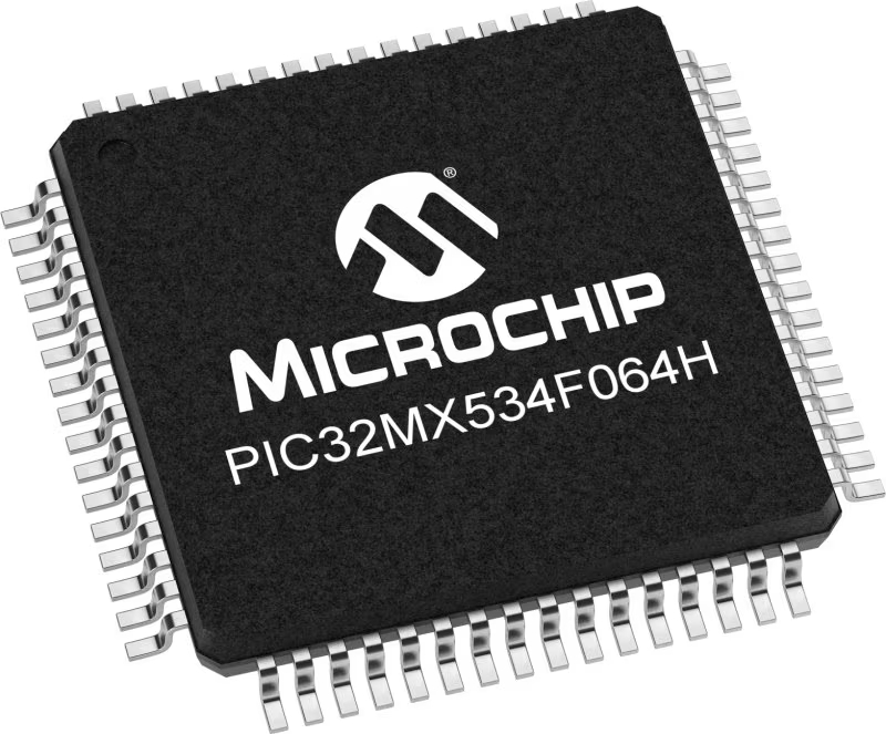
MCU
PIC32MX534F064H
Ready to take on even the most demanding designs? Our high-performance ADC is up to the challenge!
A
A
Hardware Overview
How does it work?
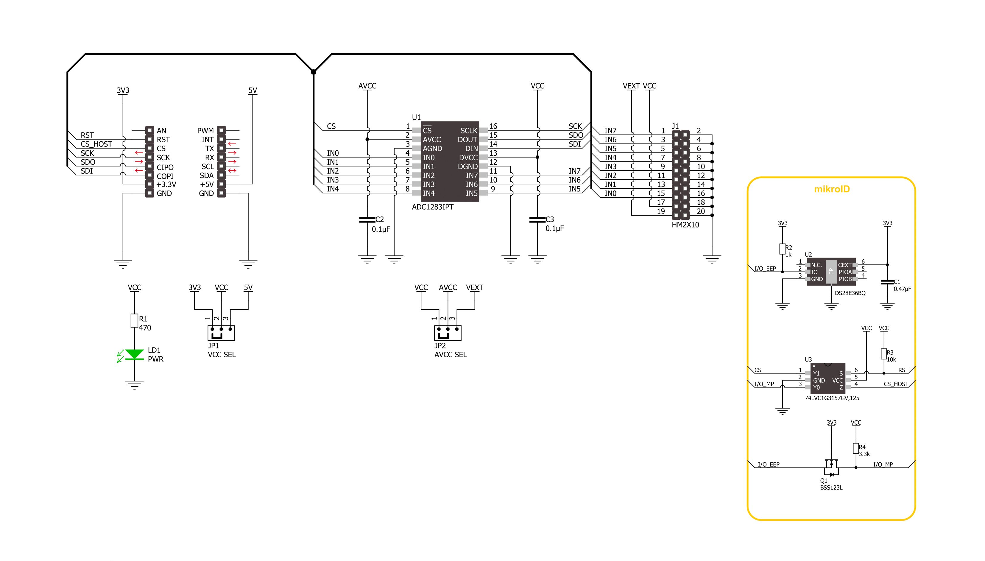
ADC 21 Click is based on the ADC1283, a high-performance eight-channel analog-to-digital converter from STMicroelectronics. The ADC1283 implements a successive approximation register (SAR) structure to convert analog signals into 12-bit pure binary digital outputs. The conversion circuit includes a fast settling time comparator to convey instruction into the register to store digital 0 or 1 and a redistribution DAC with logic control to have the ADC compare the track signal with a reference signal at each clock cycle. ADC 21 Click communicates with MCU through a standard SPI interface and operates at clock rates up to 3.2MHz,
for all configurations and acquiring conversion results. The AD conversion is carried out in two phases. The sampling phase conveys the input signal through the capacitance array for the first three clock cycles, and then, the evaluation phase performs the conversion into a digital 12-bit signal within 13 clock cycles. At each clock cycle of the evaluation phase, the hold signal is compared with a new value distributed by the DAC, and the result is stored in the 12-bit register, with MSB first. A complete conversion requires 16 clock cycles to generate a new 12-bit word on the SDO pin on the mikroBUS™ socket. This Click board™ can operate with
either 3.3V or 5V logic voltage levels selected via the VCC SEL jumper. This way, it is allowed for both 3.3V and 5V capable MCUs to use the communication lines properly. Additionally, there is a possibility for the ADC1283 analog power supply selection via jumper labeled AVCC SEL to supply the ADC1283 from an external power supply, in the range from 2.7V to 5.5V or with mikroBUS™ power rails. However, the Click board™ comes equipped with a library containing easy-to-use functions and an example code that can be used, as a reference, for further development.

Features overview
Development board
PIC32MX Clicker is a compact starter development board that brings the flexibility of add-on Click boards™ to your favorite microcontroller, making it a perfect starter kit for implementing your ideas. It comes with an onboard 32-bit PIC32 microcontroller, the PIC32MX534F064H from Microchip, a USB connector, LED indicators, buttons, a mikroProg connector, and a header for interfacing with external electronics. Thanks to its compact design with clear and easy-recognizable silkscreen markings, it provides a fluid and immersive working experience, allowing access
anywhere and under any circumstances. Each part of the PIC32MX Clicker development kit contains the components necessary for the most efficient operation of the same board. In addition to the possibility of choosing the PIC32MX Clicker programming method, using USB HID mikroBootloader, or through an external mikroProg connector for PIC, dsPIC, or PIC32 programmer, the Clicker board also includes a clean and regulated power supply module for the development kit. The USB Mini-B connection can provide up to 500mA of current, which is more
than enough to operate all onboard and additional modules. All communication methods that mikroBUS™ itself supports are on this board, including the well-established mikroBUS™ socket, reset button, and several buttons and LED indicators. PIC32MX Clicker is an integral part of the Mikroe ecosystem, allowing you to create a new application in minutes. Natively supported by Mikroe software tools, it covers many aspects of prototyping thanks to a considerable number of different Click boards™ (over a thousand boards), the number of which is growing every day.

Microcontroller Overview
MCU Card / MCU
Architecture
PIC32
MCU Memory (KB)
64
Silicon Vendor
Microchip
Pin count
64
RAM (Bytes)
16384
Used MCU Pins
mikroBUS™ mapper
Take a closer look
Click board™ Schematic
Step by step
Project assembly

Start by selecting your development board and Click board™. Begin with the PIC32MX clicker as your development board.


Software Support
Library Description
This library contains API for ADC 21 Click driver.
Key functions:
adc21_read_raw_adcThis function reads raw ADC value from the selected channel by using SPI serial interface.adc21_read_voltageThis function reads raw ADC value from the selected channel and converts it to proportional voltage level depending on the AVCC selection.
Open Source
Code example
The complete application code and a ready-to-use project are available through the NECTO Studio Package Manager for direct installation in the NECTO Studio. The application code can also be found on the MIKROE GitHub account.
/*!
 * @file main.c
 * @brief ADC 21 Click example
 *
 * # Description
 * This example demonstrates the use of ADC 21 Click board by reading and displaying
 * the voltage levels from 8 analog input channels.
 *
 * The demo application is composed of two sections :
 *
 * ## Application Init
 * Initializes the driver and logger.
 *
 * ## Application Task
 * Reads the voltage levels from all 8 analog input channels and displays the results
 * on the USB UART once per second approximately.
 *
 * @author Stefan Filipovic
 *
 */

#include "board.h"
#include "log.h"
#include "adc21.h"

static adc21_t adc21;
static log_t logger;

void application_init ( void )
{
    log_cfg_t log_cfg;  /**< Logger config object. */
    adc21_cfg_t adc21_cfg;  /**< Click config object. */

    /**
     * Logger initialization.
     * Default baud rate: 115200
     * Default log level: LOG_LEVEL_DEBUG
     * @note If USB_UART_RX and USB_UART_TX
     * are defined as HAL_PIN_NC, you will
     * need to define them manually for log to work.
     * See @b LOG_MAP_USB_UART macro definition for detailed explanation.
     */
    LOG_MAP_USB_UART( log_cfg );
    log_init( &logger, &log_cfg );
    log_info( &logger, " Application Init " );

    // Click initialization.
    adc21_cfg_setup( &adc21_cfg );
    ADC21_MAP_MIKROBUS( adc21_cfg, MIKROBUS_1 );
    if ( SPI_MASTER_ERROR == adc21_init( &adc21, &adc21_cfg ) )
    {
        log_error( &logger, " Communication init." );
        for ( ; ; );
    }

    log_info( &logger, " Application Task " );
}

void application_task ( void )
{
    static uint8_t ch_num = ADC21_CHANNEL_0;
    float ch_voltage;
    if ( ADC21_OK == adc21_read_voltage ( &adc21, ch_num, ADC21_AVCC_3V3, &ch_voltage ) )
    {
        log_printf ( &logger, " CH%u voltage: %.2f V\r\n", ( uint16_t ) ch_num, ch_voltage );
    }
    if ( ++ch_num > ADC21_CHANNEL_7 )
    {
        log_printf ( &logger, " ------------------------\r\n\n" );
        ch_num = ADC21_CHANNEL_0;
        Delay_ms ( 1000 );
    }
}

int main ( void )
{
    /* Do not remove this line or clock might not be set correctly. */
    #ifdef PREINIT_SUPPORTED
    preinit();
    #endif

    application_init( );

    for ( ; ; )
    {
        application_task( );
    }

    return 0;
}

// ------------------------------------------------------------------------ END


