Achieve seamless integration and unleash limitless creativity with our Shuttle board and ATmega6450
Expand. Enhance. Excel.

Published Nov 07, 2023
Click board™
Shuttle Click
Dev. board
EasyAVR PRO v8
Compiler
NECTO Studio
MCU
ATmega6450
Unlock infinite possibilities by seamlessly expanding your development platform's capabilities
A
A
Hardware Overview
How does it work?
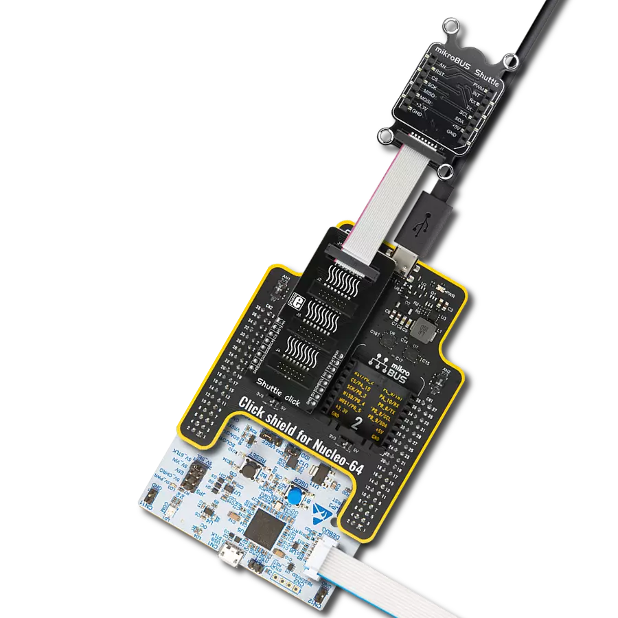
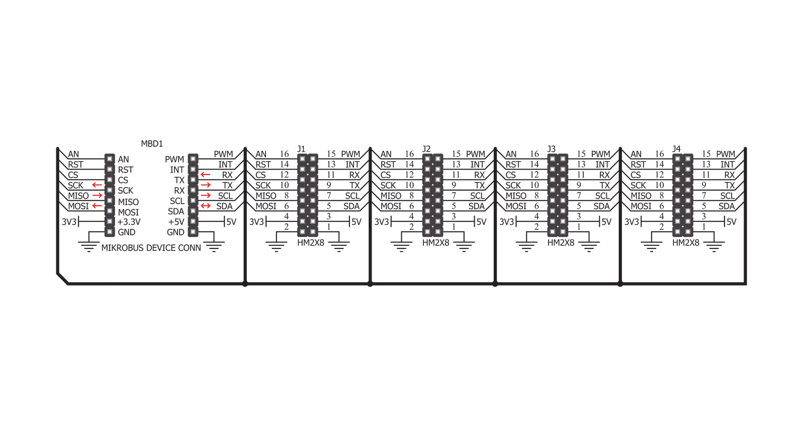
Shuttle Click consists of a high-quality PCB that can be connected to the mikroBUS™ as any other click board. The central part of the Shuttle click is populated with the four ICD BOX headers. Each of these four headers is connected to the same type of header on the add-on board, also known as mikroBUS Shuttle, by a flat ribbon cable. Thanks to the ICD BOX headers, the connection remains firm and stable. Besides the ICD BOX headers, these mikroBUS Shuttle add-on boards also have one mikroBUS™ equipped so that the click board can be securely fitted to it. This stacking topology allows for easy manipulation and reconfiguration of the stacked click boards™, retaining a perfect connection quality at all times. When there's a need to expand the development system with even more mikroBUS™ slots, one of the free
mikroBUS shuttles can be populated with yet another Shuttle Click, allowing even more connections. This makes the stacking capacity almost unlimited. However, attention should be paid not to make mikroBUS™ lines too long. In situations like this, the frequency of the communication might need to be stepped down a bit to compensate for the longer mikroBUS™ signal lines. Lines of the mikroBUS™ to which Shuttle click is attached are shared through all four ICD BOX headers - each of the four ICD BOX 2x8 pin headers mirrors pins of the connected mikroBUS™. Therefore, each mikroBUS Shuttle add-on board shares the same mikroBUS™ pins as the other mikroBUS Shuttles connected to the same Shuttle click. For this reason, extra care should be taken when working with click boards™
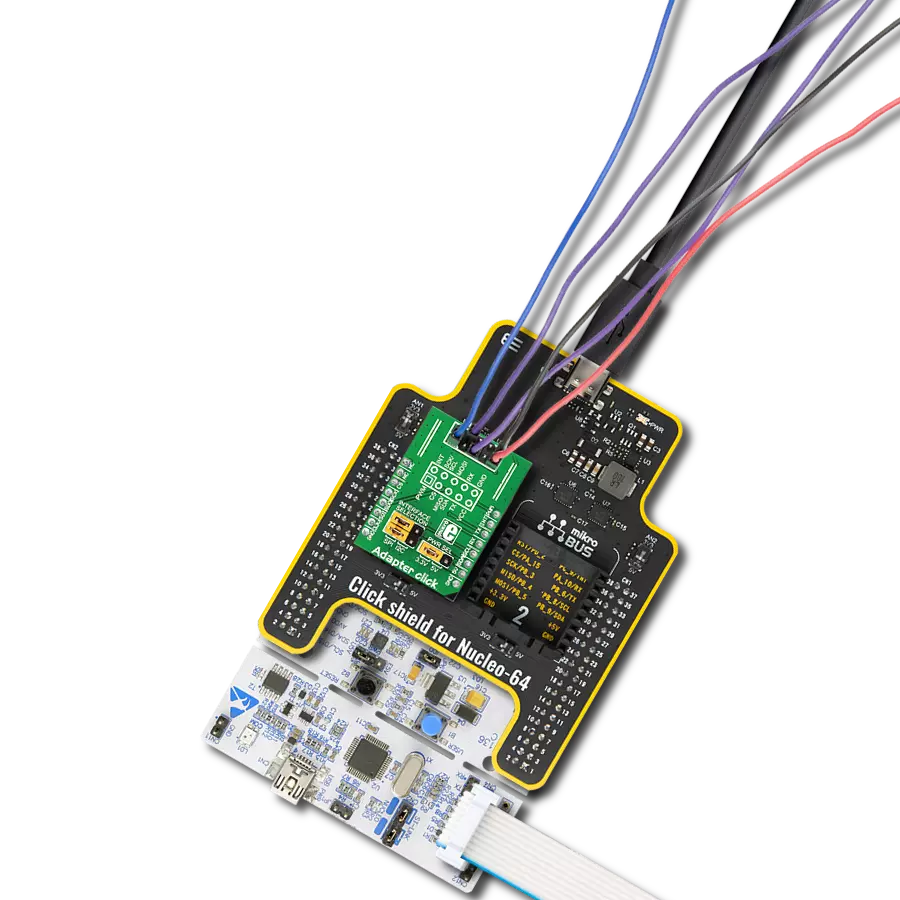
that share the same pins on the mikroBUS™, either for communication (SPI, UART, I2C) or for some other purpose (RST, INT, or other pins used as GPIO). For example, I2C and 1-Wire protocols are designed with stacking in mind, so the collision avoidance mechanisms are already in place for these protocols. It is enough to change the slave address of the click board™, and data collision won't be a problem anymore, even while sharing the same pins for communication. Also, since all the stacked click boards™ share the same power rails, care should be taken when combining click boards™ with significant power consumption. The power consumption from all the click boards™ combined should not exceed the maximum power a development system can deliver.

Features overview
Development board
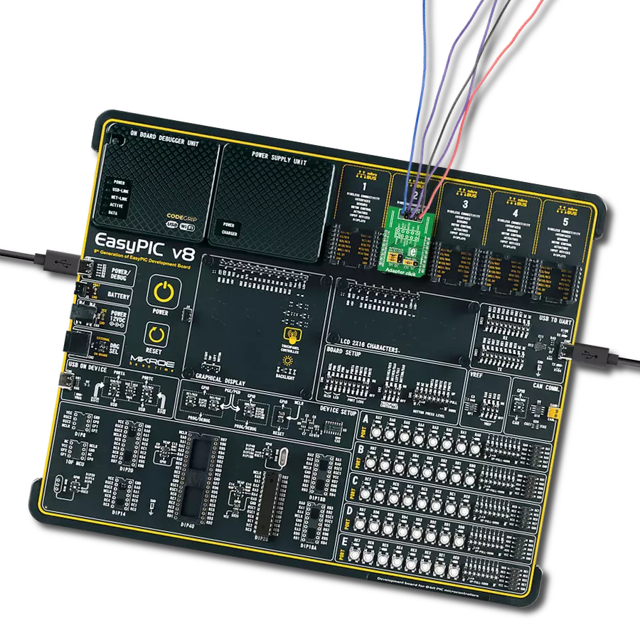
EasyAVR PRO v8 is a development board specially designed for the needs of rapid development of embedded applications. It supports a wide range of microcontrollers, such as different 8/16-bit AVR® MCUs from Microchip, regardless of their number of pins, and a broad set of unique functions, such as the first-ever embedded debugger/programmer over a WiFi network. The development board is well organized and designed so that the end-user has all the necessary elements, such as switches, buttons, indicators, connectors, and others, in one place. Thanks to innovative manufacturing technology, EasyAVR PRO v8 provides a fluid and immersive working experience, allowing access
anywhere and under any circumstances at any time. Each part of the EasyAVR PRO v8 development board contains the components necessary for the most efficient operation of the same board. An advanced integrated CODEGRIP programmer/debugger module offers many valuable programming/debugging options, including support for JTAG, SWD, and SWO Trace (Single Wire Output)), and seamless integration with the Mikroe software environment. Besides, it also includes a clean and regulated power supply module for the development board. It can use a wide range of external power sources, including a battery, an external 12V power supply, and a power source via
the USB Type-C (USB-C) connector. Communication options such as USB-UART and USB DEVICE are also included, alongside the well-established mikroBUS™ standard, a standardized socket for the MCU card (SiBRAIN standard), and two display options for the TFT board line of products and character-based LCD. EasyAVR PRO v8 is an integral part of the Mikroe ecosystem for rapid development. Natively supported by Mikroe software tools, it covers many aspects of prototyping and development thanks to a considerable number of different Click boards™ (over a thousand boards), the number of which is growing every day.

Microcontroller Overview
MCU Card / MCU
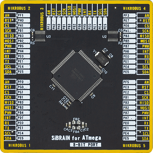
Type
8th Generation
Architecture
AVR
MCU Memory (KB)
64
Silicon Vendor
Microchip
Pin count
100
RAM (Bytes)
4096
Used MCU Pins
mikroBUS™ mapper
Take a closer look
Click board™ Schematic
Step by step
Project assembly

Start by selecting your development board and Click board™. Begin with the EasyAVR PRO v8 as your development board.


Track your results in real time
Application Output
1. Application Output - In Debug mode, the 'Application Output' window enables real-time data monitoring, offering direct insight into execution results. Ensure proper data display by configuring the environment correctly using the provided tutorial.

2. UART Terminal - Use the UART Terminal to monitor data transmission via a USB to UART converter, allowing direct communication between the Click board™ and your development system. Configure the baud rate and other serial settings according to your project's requirements to ensure proper functionality. For step-by-step setup instructions, refer to the provided tutorial.

3. Plot Output - The Plot feature offers a powerful way to visualize real-time sensor data, enabling trend analysis, debugging, and comparison of multiple data points. To set it up correctly, follow the provided tutorial, which includes a step-by-step example of using the Plot feature to display Click board™ readings. To use the Plot feature in your code, use the function: plot(*insert_graph_name*, variable_name);. This is a general format, and it is up to the user to replace 'insert_graph_name' with the actual graph name and 'variable_name' with the parameter to be displayed.

Software Support
Library Description
This library contains API for Shuttle Click driver.
Key functions:
shuttle_set_pin_high- This function sets the output voltage on the specified pin to high.shuttle_set_pin_low- This function sets the output voltage on the specified pin to low.
Open Source
Code example
The complete application code and a ready-to-use project are available through the NECTO Studio Package Manager for direct installation in the NECTO Studio. The application code can also be found on the MIKROE GitHub account.
/*!
 * \file
 * \brief Shuttle Click example
 *
 * # Description
 * This example showcases how to initialize, configure and use the Terminal Click. It is a simple
 * GPIO Click which uses high-quality PCB design, four ICD BOX headers and flat ribbon cables to
 * enable stable communication and easy stacking of other Click modules.
 *
 * The demo application is composed of two sections :
 *
 * ## Application Init
 * This function initializes and configures the Click and logger modules.
 *
 * ## Application Task
 * This function sets the output on all the pins (one by one) on the left side to high, going
 * from top to bottom and then does the same with the ones on the right side, after which it
 * sets all pins to high and after one second sets them back to low.
 *
 * \author MikroE Team
 *
 */
// ------------------------------------------------------------------- INCLUDES

#include "board.h"
#include "log.h"
#include "shuttle.h"

// ------------------------------------------------------------------ VARIABLES

static shuttle_t shuttle;
static log_t logger;

static digital_out_t *pin_addr[ 12 ] =
{
    &shuttle.mosi,    // 0 MOSI
    &shuttle.miso,    // 1 MISO
    &shuttle.sck,     // 2 SCK
    &shuttle.cs,      // 3 CS
    &shuttle.rst,     // 4 RST
    &shuttle.an,      // 5 AN
    &shuttle.pwm,     // 6 PWM
    &shuttle.int_pin, // 7 INT
    &shuttle.tx_pin,  // 8 TX
    &shuttle.rx_pin,  // 9 RX
    &shuttle.scl,     // 10 SCL
    &shuttle.sda      // 11 SDA
};

// ------------------------------------------------------- ADDITIONAL FUNCTIONS

static void blink ( digital_out_t *pin )
{
    shuttle_set_pin_high( pin );
    Delay_100ms( );
    shuttle_set_pin_low( pin );
}

static void all_on ( )
{
   int i;

   for( i = 0; i < 12; i++ )
   {
        shuttle_set_pin_high( pin_addr[ i ] );
   }
}

static void all_off ( )
{
   int i;

   for( i = 0; i < 12; i++ )
   {
        shuttle_set_pin_low( pin_addr[ i ] );
   }
}

// ------------------------------------------------------ APPLICATION FUNCTIONS

void application_init ( )
{
    log_cfg_t log_cfg;
    shuttle_cfg_t cfg;

    /**
     * Logger initialization.
     * Default baud rate: 115200
     * Default log level: LOG_LEVEL_DEBUG
     * @note If USB_UART_RX and USB_UART_TX
     * are defined as HAL_PIN_NC, you will
     * need to define them manually for log to work.
     * See @b LOG_MAP_USB_UART macro definition for detailed explanation.
     */
    LOG_MAP_USB_UART( log_cfg );
    log_init( &logger, &log_cfg );
    log_info(&logger, "---- Application Init ----");

    //  Click initialization.

    shuttle_cfg_setup( &cfg );
    SHUTTLE_MAP_MIKROBUS( cfg, MIKROBUS_1 );
    shuttle_init( &shuttle, &cfg );
}

void application_task ( )
{
    int i;

    for( i = 0; i < 12; i++ )
    {
        blink( pin_addr[ i ] );
    }

    all_on( );
    Delay_1sec( );
    all_off( );
}

int main ( void )
{
    /* Do not remove this line or clock might not be set correctly. */
    #ifdef PREINIT_SUPPORTED
    preinit();
    #endif

    application_init( );

    for ( ; ; )
    {
        application_task( );
    }

    return 0;
}

// ------------------------------------------------------------------------ END