Create a data acquisition system with ADAQ4003 and MK64FN1M0VDC12
Capture, digitize, and analyze data

Published Jun 01, 2023
Click board™
DAQ 3 Click
Dev. board
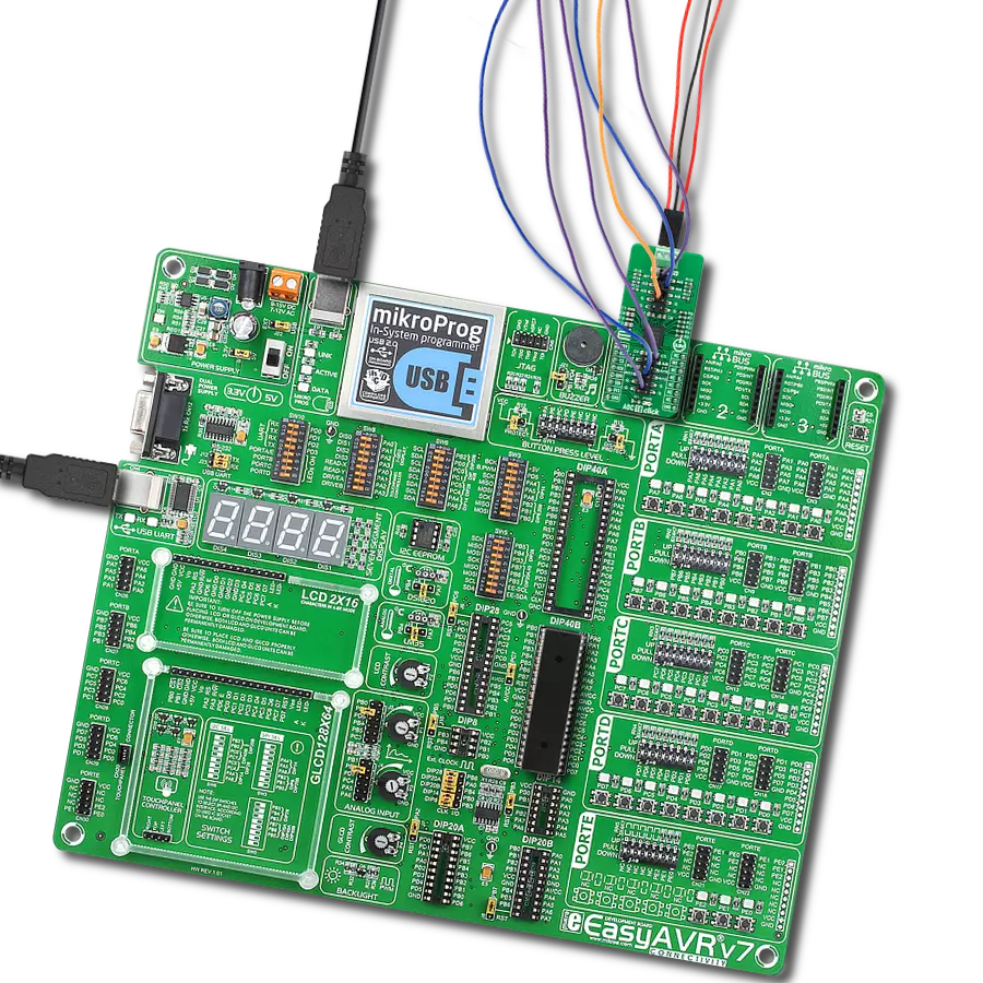
Clicker 2 for Kinetis
Compiler
NECTO Studio
MCU
MK64FN1M0VDC12
Unlock the power of data with our cutting-edge data acquisition (DAQ) solution empowering real-time monitoring, precise measurements, and data-driven decision-making
A
A
Hardware Overview
How does it work?
DAQ 3 Click is based on the ADAQ4003, a fast and precise system-in-package DAQ signal chain solution from Analog Devices. This μModule combines multiple standard signal processing and conditioning blocks into a single device containing a high bandwidth fully differential ADC driver, a low noise reference buffer, an 18-bit SAR ADC, and selectable gain options. It can convert 2,000,000 samples per second (2 MSPS), achieving a high degree of specified accuracy. The ADAQ4003 also has a valid first conversion after being powered down for long periods to reduce the power consumed in applications where the ADC does not convert constantly. The ADAQ4003 requires a supply voltage of 1.8V to work regularly. Therefore, a small regulating LDO, the ADP151 from Analog Devices, provides a 1.8V out of mikroBUS™ rails. In combination with LT3032, dual low noise positive and negative low drop-out voltage linear regulator, it can generate regulated ±15V positive and negative rails for any additional signal conditioning. This Click board™ also includes the LT6656, a precise voltage regulator that provides low noise and a low drop-out voltage reference of 4.096V. This feature intends to optimally
drive the dynamic input impedance ofthe SAR ADC reference node. DAQ 3 Click communicates with MCU using the 16-bit SPI serial interface compatible with standard SPI, QSPI™, MICROWIRE™, and digital signal processors (DSPs). The ADAQ4003 also has a Turbo mode allowing a slower SPI clock rate, simplifying interfacing. Turbo mode activates by writing to the configuration register and replaces the busy indicator feature when enabled. The ADAQ4003 can achieve the maximum throughput of 2MSPS only with enabled Turbo mode and a minimum clock rate of 75MHz. An additional feature of this Click board™ represents specific settings related to a fully differential ADC driver like Power-Down Reference Buffer and Amplifier labeled as DRE and DAM routed on the RST and AN pins of the mikroBUS™ socket. Also, the ADC driver has one power mode pin labeled as MOD and routed on the PWM pin of the mikroBUS™ socket, which enables the full performance of the driver with this pin set to its high logic state. On the other hand, the ADAQ4003 also uses an INT pin as an interrupt, indicating that the conversion result is available on the SDO line of the SPI interface. This Click board™ also comes with the
jumpers labeled from JP2-JP8 required to achieve optimized performance with selectable gain options of 0.454, 0.909, 1, or 1.9. With jumpers labeled as JP4 and JP7 populated on the board, the default gain of the ADAQ4003 is set to 1. Please consult the attached datasheet for more information about the correct jumper configuration when selecting gain. DAQ 3 Click possesses two SMA connectors labeled IN- and IN+, providing low-noise analog signal sources. These inputs are fed and buffered with the LTC6373, a precision instrumentation amplifier with fully differential outputs that achieve excellent offset voltage, gain error, gain drift, and gain non-linearity. The user can easily program the gain to one of seven available settings through 3 slide switches labeled GAIN SEL. This Click board™ can operate with either 3.3V or 5V logic voltage levels selected via the VIO SEL jumper. This way, both 3.3V and 5V capable MCUs can use the communication lines properly. However, the Click board™ comes equipped with a library containing easy-to-use functions and an example code that can be used, as a reference, for further development.

Features overview
Development board
Clicker 2 for Kinetis is a compact starter development board that brings the flexibility of add-on Click boards™ to your favorite microcontroller, making it a perfect starter kit for implementing your ideas. It comes with an onboard 32-bit ARM Cortex-M4F microcontroller, the MK64FN1M0VDC12 from NXP Semiconductors, two mikroBUS™ sockets for Click board™ connectivity, a USB connector, LED indicators, buttons, a JTAG programmer connector, and two 26-pin headers for interfacing with external electronics. Its compact design with clear and easily recognizable silkscreen markings allows you to build gadgets with unique functionalities and
features quickly. Each part of the Clicker 2 for Kinetis development kit contains the components necessary for the most efficient operation of the same board. In addition to the possibility of choosing the Clicker 2 for Kinetis programming method, using a USB HID mikroBootloader or an external mikroProg connector for Kinetis programmer, the Clicker 2 board also includes a clean and regulated power supply module for the development kit. It provides two ways of board-powering; through the USB Micro-B cable, where onboard voltage regulators provide the appropriate voltage levels to each component on the board, or
using a Li-Polymer battery via an onboard battery connector. All communication methods that mikroBUS™ itself supports are on this board, including the well-established mikroBUS™ socket, reset button, and several user-configurable buttons and LED indicators. Clicker 2 for Kinetis is an integral part of the Mikroe ecosystem, allowing you to create a new application in minutes. Natively supported by Mikroe software tools, it covers many aspects of prototyping thanks to a considerable number of different Click boards™ (over a thousand boards), the number of which is growing every day.

Microcontroller Overview
MCU Card / MCU

Architecture
ARM Cortex-M4
MCU Memory (KB)
1024
Silicon Vendor
NXP
Pin count
121
RAM (Bytes)
262144
Used MCU Pins
mikroBUS™ mapper
Take a closer look
Click board™ Schematic

Step by step
Project assembly

Start by selecting your development board and Click board™. Begin with the Clicker 2 for Kinetis as your development board.


Track your results in real time
Application Output
1. Application Output - In Debug mode, the 'Application Output' window enables real-time data monitoring, offering direct insight into execution results. Ensure proper data display by configuring the environment correctly using the provided tutorial.

2. UART Terminal - Use the UART Terminal to monitor data transmission via a USB to UART converter, allowing direct communication between the Click board™ and your development system. Configure the baud rate and other serial settings according to your project's requirements to ensure proper functionality. For step-by-step setup instructions, refer to the provided tutorial.

3. Plot Output - The Plot feature offers a powerful way to visualize real-time sensor data, enabling trend analysis, debugging, and comparison of multiple data points. To set it up correctly, follow the provided tutorial, which includes a step-by-step example of using the Plot feature to display Click board™ readings. To use the Plot feature in your code, use the function: plot(*insert_graph_name*, variable_name);. This is a general format, and it is up to the user to replace 'insert_graph_name' with the actual graph name and 'variable_name' with the parameter to be displayed.

Software Support
Library Description
This library contains API for DAQ 3 Click driver.
Key functions:
float daq3_get_voltage ( daq3_t *ctx );DAQ 3 get voltage function.int32_t daq3_get_conversion_result ( daq3_t *ctx, daq3_reg_cfg_t cfg_data );DAQ 3 get conversion result function.err_t daq3_generic_read ( daq3_t *ctx, uint8_t reg, uint8_t *data_out );DAQ 3 data reading function.
Open Source
Code example
The complete application code and a ready-to-use project are available through the NECTO Studio Package Manager for direct installation in the NECTO Studio. The application code can also be found on the MIKROE GitHub account.
/*!
 * @file main.c
 * @brief Daq3 Click example
 *
 * # Description
 * The demo application reads ADC value, calculate and display voltage ( mV ).
 *
 * The demo application is composed of two sections :
 *
 * ## Application Init
 * Initializes SPI driver and start to write log.
 *
 * ## Application Task
 * This is an example that demonstrates the use of the DAQ 3 click board.
 * In this example, we read ADC value, calculate and display the voltage ( mV ) data.
 * The maximum output voltage ( Vout ) is 4V and
 * depends on the gain that is set at the click.
 * The formula used to calculate is Vin = Vout / gain.
 * Keep in mind that Vout should not exceed 4V.
 * For example, if the gain is set to 2 the maximum Vin is 2V ( 2V = 4V / 2 ).
 * Results are being sent to the Usart Terminal where you can track their changes.
 *
 * @author Nenad Filipovic
 *
 */

#include "board.h"
#include "log.h"
#include "daq3.h"

static daq3_t daq3;
static log_t logger;

void application_init ( void ) {
    log_cfg_t log_cfg;    /**< Logger config object. */
    daq3_cfg_t daq3_cfg;  /**< Click config object. */

    /**
     * Logger initialization.
     * Default baud rate: 115200
     * Default log level: LOG_LEVEL_DEBUG
     * @note If USB_UART_RX and USB_UART_TX
     * are defined as HAL_PIN_NC, you will
     * need to define them manually for log to work.
     * See @b LOG_MAP_USB_UART macro definition for detailed explanation.
     */
    LOG_MAP_USB_UART( log_cfg );
    log_init( &logger, &log_cfg );
    log_printf( &logger, "\r\n" );
    log_info( &logger, " Application Init " );

    // Click initialization.

    daq3_cfg_setup( &daq3_cfg );
    DAQ3_MAP_MIKROBUS( daq3_cfg, MIKROBUS_1 );
    err_t init_flag  = daq3_init( &daq3, &daq3_cfg );
    if ( init_flag == SPI_MASTER_ERROR ) {
        log_error( &logger, " Application Init Error. " );
        log_info( &logger, " Please, run program again... " );

        for ( ; ; );
    }

    daq3_default_cfg ( &daq3 );
    log_info( &logger, " Application Task \r\n" );
    Delay_ms( 100 );
    log_printf( &logger, "---------------------------\r\n" );
    log_printf( &logger, "         DAQ 3 click       \r\n" );
    log_printf( &logger, "---------------------------\r\n" );
}

void application_task ( void ) {
    float voltage = daq3_get_voltage( &daq3 );
    log_printf( &logger, "   Voltage : %.3f mV       \r\n", voltage );
    log_printf( &logger, "---------------------------\r\n" );
    Delay_ms( 2000 );
}

void main ( void ) {
    application_init( );

    for ( ; ; ) {
        application_task( );
    }
}

// ------------------------------------------------------------------------ END