Efficiently manage and retrieve your data with GD25LQ16C and MK64FN1M0VDC12
Revolutionize your storage solution

Published Aug 29, 2023
Click board™
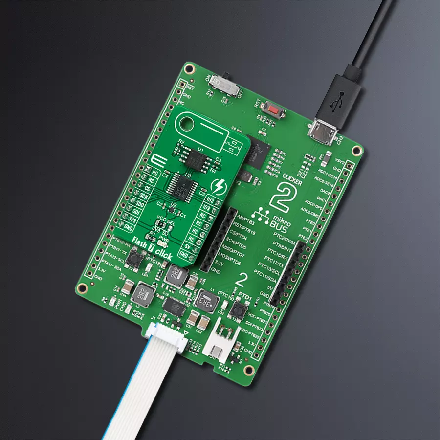
Flash 7 Click
Dev. board
Clicker 2 for Kinetis
Compiler
NECTO Studio
MCU
MK64FN1M0VDC12
Enjoy rapid file transfers and smoother application performance
A
A
Hardware Overview
How does it work?
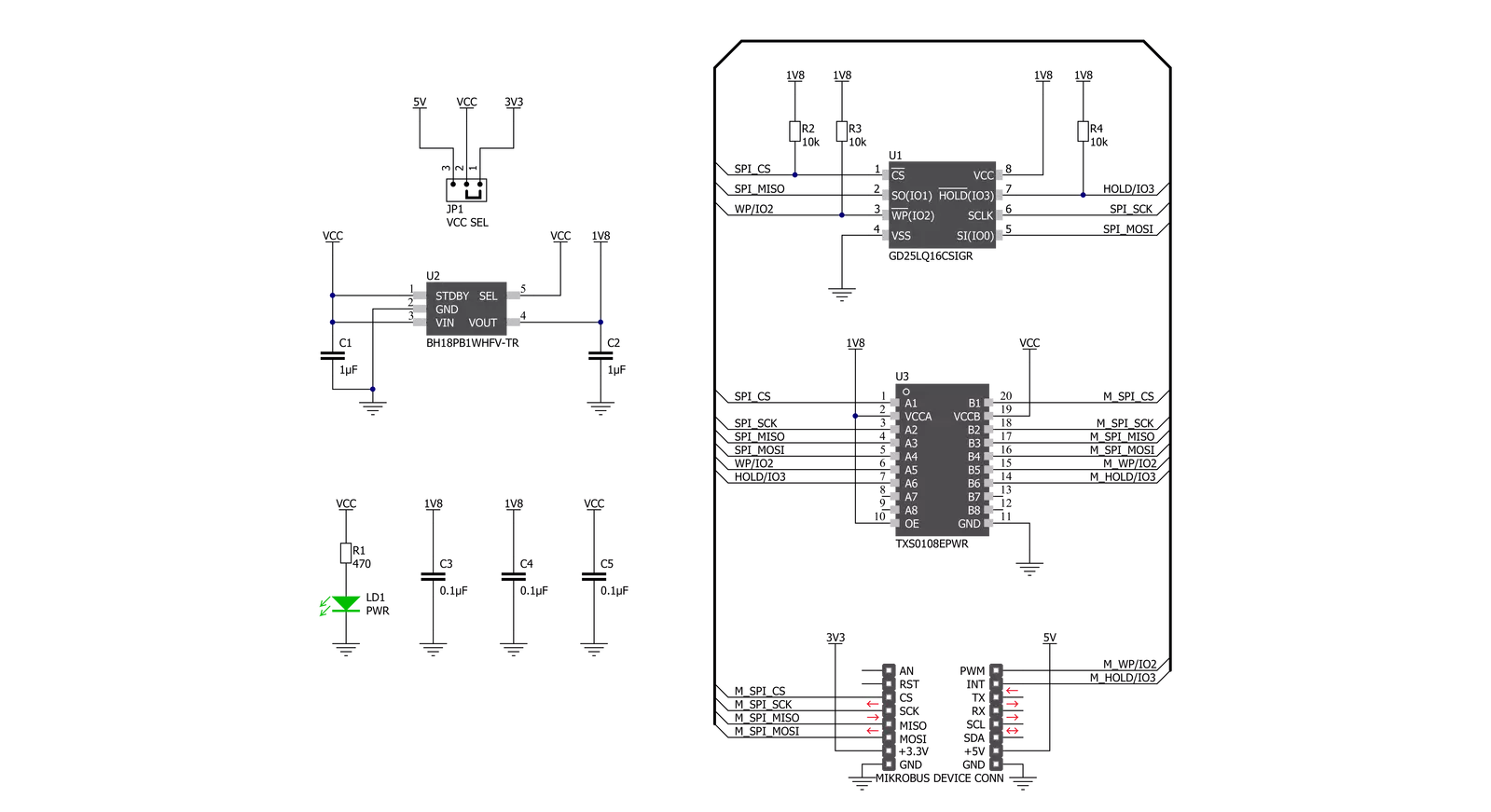
Flash 7 Click is based on the GD25LQ16C, a high-performance 16Mbit SPI NOR Flash Memory solution with advanced security features from GigaDevice Semiconductor. Requiring only six signals to communicate between the MCU and the memory thus reduces the design complexity board space and total system cost. It is specifically designed to meet the different needs of various electronic applications in terms of density, performance, reliability, and security while providing low power consumption. This Click board™ includes an LDO regulator BH18PB1WHFV from Rohm Semiconductor to provide the 1.8 V supply voltage. The LDO cuts power consumption by lowering its current consumption to approximately 2 μA when the application operates in the standby state. The output from the LDO
regulator provides a needed reference voltage for one side of the TXS0108E, an 8-bit bidirectional level shifting, and a voltage translator for open-drain and push-pull applications from Texas Instruments. The reference voltage for the other side of the level shifter is taken from the 3.3V pin from the mikroBUS™. Flash 7 Click communicates with MCU using the SPI serial interface that supports the Dual/Quad SPI and the two most common modes, SPI Mode 0 and 3, with a maximum SPI frequency of 104 MHz. The Dual I/O data is transferred with a speed of 208 Mbits/s, and the Quad I/O data with a speed of 416 Mbits/s. In addition to the SPI communication, the Flash 7 Click has two additional pins for Write Protection and HOLD function routed to the PWM and INT pins of the mikroBUS™ socket. The HOLD
pin, labeled as IO3, can be used to pause the serial communication with the device without stopping the operation of the write status register, programming, or erasing in progress. The configurable Write Protection function IO2 protects the memory array contents via the Software Protection Mode. This Click board™ can operate with either 3.3V or 5V logic voltage levels selected via the VCC SEL jumper. This way, both 3.3V and 5V capable MCUs can use the communication lines properly. Also, this Click board™ comes equipped with a library containing easy-to-use functions and an example code that can be used as a reference for further development.


Features overview
Development board
Clicker 2 for Kinetis is a compact starter development board that brings the flexibility of add-on Click boards™ to your favorite microcontroller, making it a perfect starter kit for implementing your ideas. It comes with an onboard 32-bit ARM Cortex-M4F microcontroller, the MK64FN1M0VDC12 from NXP Semiconductors, two mikroBUS™ sockets for Click board™ connectivity, a USB connector, LED indicators, buttons, a JTAG programmer connector, and two 26-pin headers for interfacing with external electronics. Its compact design with clear and easily recognizable silkscreen markings allows you to build gadgets with unique functionalities and
features quickly. Each part of the Clicker 2 for Kinetis development kit contains the components necessary for the most efficient operation of the same board. In addition to the possibility of choosing the Clicker 2 for Kinetis programming method, using a USB HID mikroBootloader or an external mikroProg connector for Kinetis programmer, the Clicker 2 board also includes a clean and regulated power supply module for the development kit. It provides two ways of board-powering; through the USB Micro-B cable, where onboard voltage regulators provide the appropriate voltage levels to each component on the board, or
using a Li-Polymer battery via an onboard battery connector. All communication methods that mikroBUS™ itself supports are on this board, including the well-established mikroBUS™ socket, reset button, and several user-configurable buttons and LED indicators. Clicker 2 for Kinetis is an integral part of the Mikroe ecosystem, allowing you to create a new application in minutes. Natively supported by Mikroe software tools, it covers many aspects of prototyping thanks to a considerable number of different Click boards™ (over a thousand boards), the number of which is growing every day.

Microcontroller Overview
MCU Card / MCU

Architecture
ARM Cortex-M4
MCU Memory (KB)
1024
Silicon Vendor
NXP
Pin count
121
RAM (Bytes)
262144
Used MCU Pins
mikroBUS™ mapper
Take a closer look
Click board™ Schematic
Step by step
Project assembly

Start by selecting your development board and Click board™. Begin with the Clicker 2 for Kinetis as your development board.


Software Support
Library Description
This library contains API for Flash 7 Click driver.
Key functions:
flash7_send_command- Send command functionflash7_page_program- Page program functionflash7_read_memory- Read memory function.
Open Source
Code example
The complete application code and a ready-to-use project are available through the NECTO Studio Package Manager for direct installation in the NECTO Studio. The application code can also be found on the MIKROE GitHub account.
/*!
 * @file main.c
 * @brief Flash7 Click example
 *
 * # Description
 * This is an example that demonstrates the use
 * of the Flash 7 Click board.
 *
 * The demo application is composed of two sections :
 *
 * ## Application Init
 * Initialization driver enables SPI,
 * disables write protect and hold, performs whole chip erase,
 * targets the memory address at "4096" for page program starting point
 * and writes data which is also displayed on the log.
 *
 * ## Application Task
 * In this example, the data is read from
 * the targeted memory address. The results are being sent to the Usart Terminal.
 * This task repeats every 5 sec.
 *
 * @author Stefan Ilic
 *
 */

#include "board.h"
#include "log.h"
#include "flash7.h"

static flash7_t flash7;
static log_t logger;

static char demo_data[ 9 ] = { 'm', 'i', 'k', 'r', 'o', 'E', 13 ,10 , 0 };
static char rx_data[ 9 ];
static uint32_t memory_addr;

void application_init ( void ) {
    log_cfg_t log_cfg;  /**< Logger config object. */
    flash7_cfg_t flash7_cfg;  /**< Click config object. */

    /**
     * Logger initialization.
     * Default baud rate: 115200
     * Default log level: LOG_LEVEL_DEBUG
     * @note If USB_UART_RX and USB_UART_TX
     * are defined as HAL_PIN_NC, you will
     * need to define them manually for log to work.
     * See @b LOG_MAP_USB_UART macro definition for detailed explanation.
     */
    LOG_MAP_USB_UART( log_cfg );
    log_init( &logger, &log_cfg );
    log_info( &logger, " Application Init " );

    // Click initialization.

    flash7_cfg_setup( &flash7_cfg );
    FLASH7_MAP_MIKROBUS( flash7_cfg, MIKROBUS_1 );
    err_t init_flag  = flash7_init( &flash7, &flash7_cfg );
    if ( SPI_MASTER_ERROR == init_flag ) {
        log_error( &logger, " Application Init Error. " );
        log_info( &logger, " Please, run program again... " );

        for ( ; ; );
    }

    flash7_default_cfg ( &flash7 );

    log_printf( &logger, " ----------------------- \r\n" );
    log_printf( &logger, " Chip Erase \r\n" );
    flash7_chip_erase( &flash7 );
    Delay_ms ( 1000 );
    Delay_ms ( 1000 );
    Delay_ms ( 1000 );
    Delay_ms ( 1000 );
    Delay_ms ( 1000 );

    memory_addr = 4096;

    log_printf( &logger, " ----------------------- \r\n" );
    log_printf( &logger, " Write data : %s ", demo_data );
    log_printf( &logger, " ----------------------- \r\n" );
    flash7_page_program( &flash7, memory_addr, demo_data, 9 );
    Delay_ms ( 100 );

    log_info( &logger, " Application Task " );
    log_printf( &logger, " ----------------------- \r\n" );
}

void application_task ( void ) {
    flash7_read_memory( &flash7, memory_addr, rx_data, 9 );
    log_printf( &logger, " Read data : %s ", rx_data );
    log_printf( &logger, " ----------------------- \r\n" );
    Delay_ms ( 1000 );
    Delay_ms ( 1000 );
    Delay_ms ( 1000 );
    Delay_ms ( 1000 );
    Delay_ms ( 1000 );
}

int main ( void )
{
    /* Do not remove this line or clock might not be set correctly. */
    #ifdef PREINIT_SUPPORTED
    preinit();
    #endif

    application_init( );

    for ( ; ; )
    {
        application_task( );
    }

    return 0;
}

// ------------------------------------------------------------------------ END


