Experience efficient voltage adjustment with LM317M and MK64FN1M0VDC12
Fine-tune your electronics
Published Sep 12, 2023
Click board™
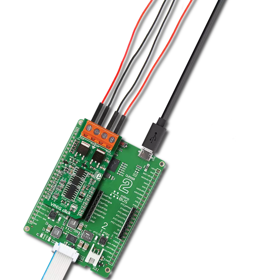
VREG Click
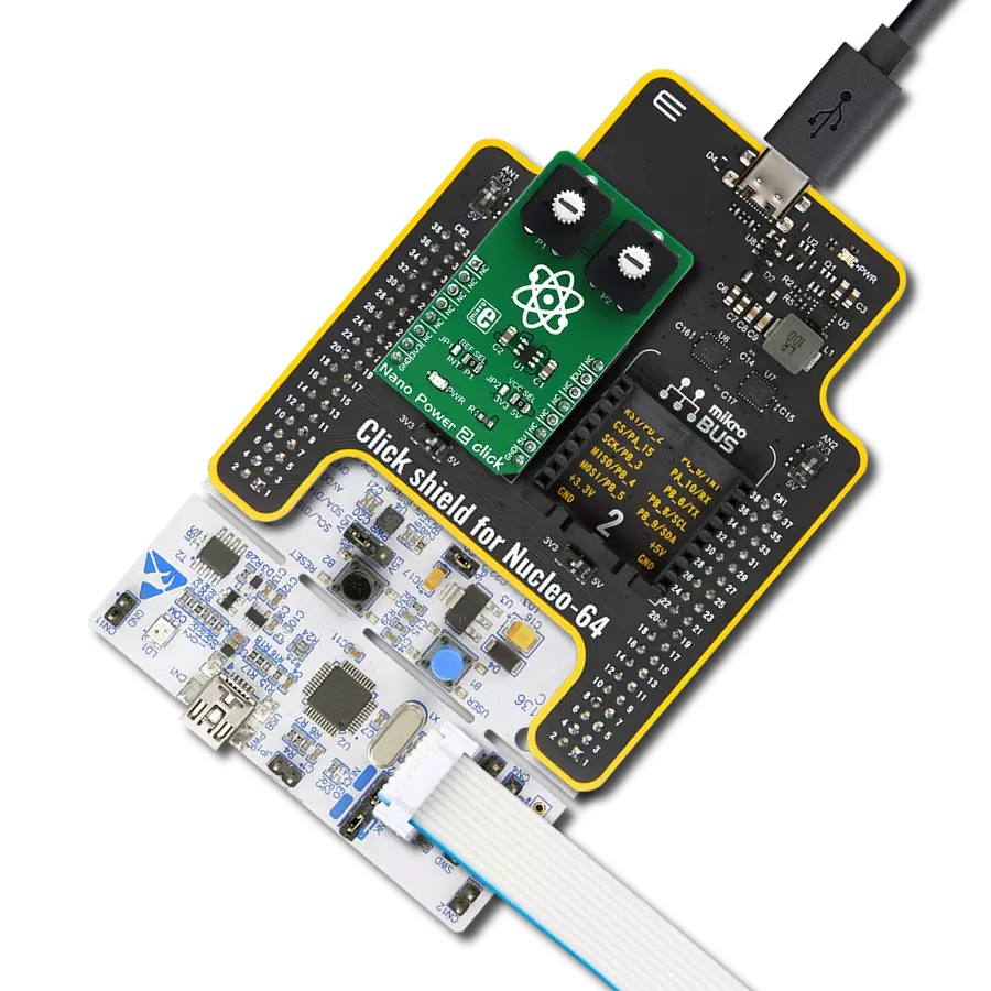
Dev. board
Clicker 2 for Kinetis
Compiler
NECTO Studio
MCU
MK64FN1M0VDC12
Our adjustable voltage regulator allows you to precisely control the output voltage, giving you the flexibility to meet your specific power requirements
A
A
Hardware Overview
How does it work?
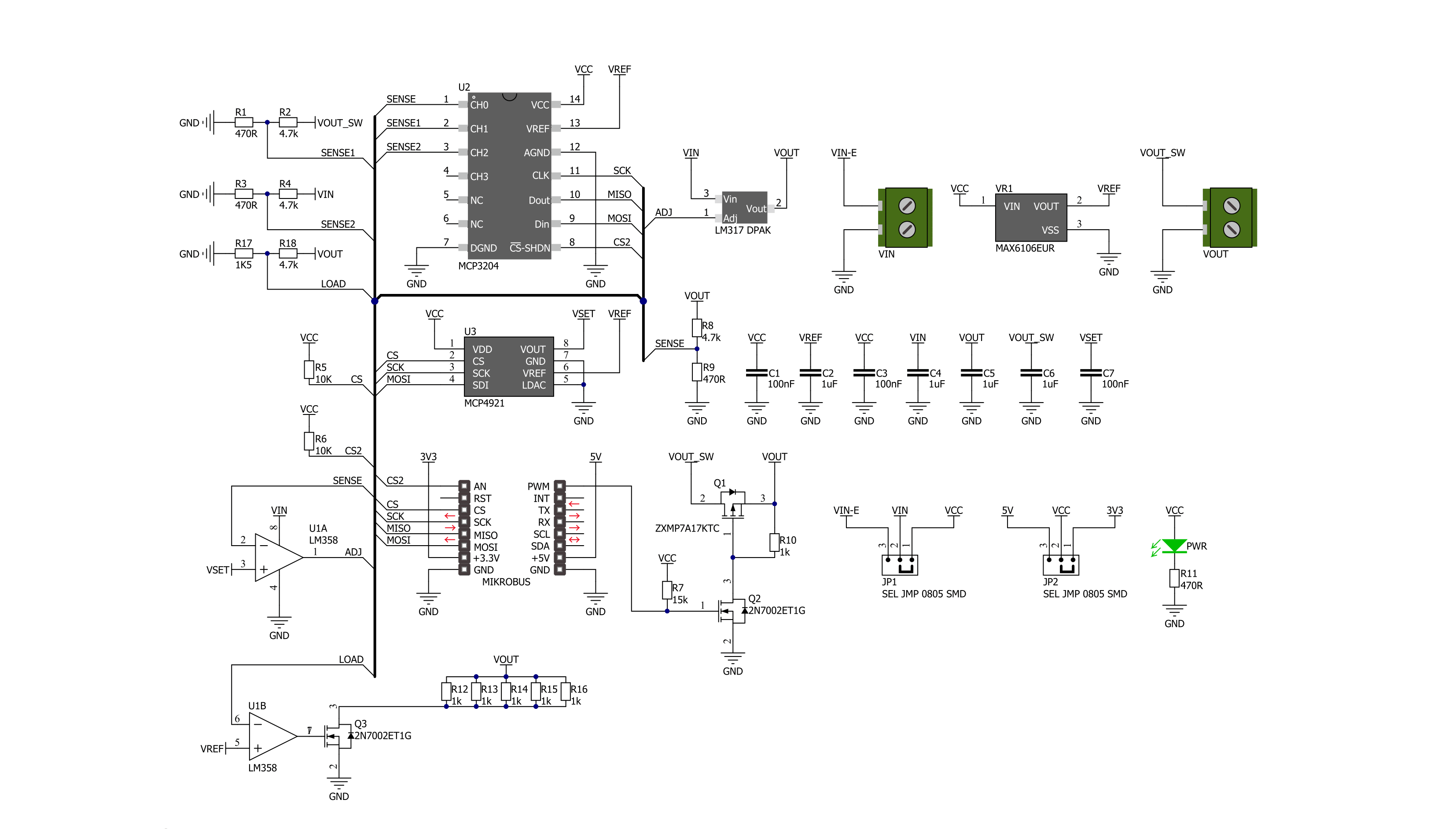
VREG Click is based on the LM317M, an adjustable voltage regulator from STMicroelectronics. It is a reliable regulator with a typical line regulation of 0.01% and load regulation of 0.1%. It also has internal short-circuit current limiting and thermal overload protection. Because of the heat dissipation while regulating the voltage, the board’s operating range is defined by two factors. The maximum input voltage and current should not exceed 20V/0.5A, and the maximum wattage arising from the current and I/O voltage difference should not exceed 1W, measured as I x (Input V – Output V). The VREG Click uses MCP3204, a 4-channel 12-bit ADC with an SPI interface from Microchip, to get the information of the output voltage of the LM317M voltage regulator, output voltage after it passes the switch MOSFET and the input voltage no matter if it is external or internal.
For that purpose, the MCP3204 uses voltage dividers. It also uses the MAX6106, a low-cost, micropower, low-dropout, high-output-current voltage reference from Analog Devices, as a 2.048V voltage reference. This Click board™ uses the MCP4921, a 12-bit DAC with an SPI interface, to set the desired voltage. This DAC includes an input amplifier, rail-to-rail amplifier, shutdown, reset-management circuitry, and a reference buffer fed by an MAX6106. The output from the DAC passes to the LM358, a low-power, dual-operational amplifier from Texas Instruments. This Op-Amp fed the LM317M voltage regulator with a precise value over the adjustment pin. This Click board™ features the ZXMP7A17K, a P-channel MOSFET from Zetex Semiconductors, as a switch to toggle the output on and off, which can be controlled over the host MCU. To communicate with the host
MCU, the VREG Click uses an SPI serial interface with separate chip select pins (CS for MCP4921 and CS2 for MCP3204). Pin SW acts as a switch over a MOSFET to toggle the output on and off. The input voltage can be used as external over the screw terminal or internal from the host board itself, depending on the set voltage over the PWR SEL selection jumper. The external and internal voltage inputs can be selected over the INPUT SEL jumper, with an external set by default. This Click board™ can operate with either 3.3V or 5V logic voltage levels selected via the PWR SEL jumper. This way, both 3.3V and 5V capable MCUs can use the communication lines properly. Also, this Click board™ comes equipped with a library containing easy-to-use functions and an example code that can be used as a reference for further development.

Features overview
Development board
Clicker 2 for Kinetis is a compact starter development board that brings the flexibility of add-on Click boards™ to your favorite microcontroller, making it a perfect starter kit for implementing your ideas. It comes with an onboard 32-bit ARM Cortex-M4F microcontroller, the MK64FN1M0VDC12 from NXP Semiconductors, two mikroBUS™ sockets for Click board™ connectivity, a USB connector, LED indicators, buttons, a JTAG programmer connector, and two 26-pin headers for interfacing with external electronics. Its compact design with clear and easily recognizable silkscreen markings allows you to build gadgets with unique functionalities and
features quickly. Each part of the Clicker 2 for Kinetis development kit contains the components necessary for the most efficient operation of the same board. In addition to the possibility of choosing the Clicker 2 for Kinetis programming method, using a USB HID mikroBootloader or an external mikroProg connector for Kinetis programmer, the Clicker 2 board also includes a clean and regulated power supply module for the development kit. It provides two ways of board-powering; through the USB Micro-B cable, where onboard voltage regulators provide the appropriate voltage levels to each component on the board, or
using a Li-Polymer battery via an onboard battery connector. All communication methods that mikroBUS™ itself supports are on this board, including the well-established mikroBUS™ socket, reset button, and several user-configurable buttons and LED indicators. Clicker 2 for Kinetis is an integral part of the Mikroe ecosystem, allowing you to create a new application in minutes. Natively supported by Mikroe software tools, it covers many aspects of prototyping thanks to a considerable number of different Click boards™ (over a thousand boards), the number of which is growing every day.

Microcontroller Overview
MCU Card / MCU

Architecture
ARM Cortex-M4
MCU Memory (KB)
1024
Silicon Vendor
NXP
Pin count
121
RAM (Bytes)
262144
Used MCU Pins
mikroBUS™ mapper
Take a closer look
Click board™ Schematic
Step by step
Project assembly

Start by selecting your development board and Click board™. Begin with the Clicker 2 for Kinetis as your development board.


Software Support
Library Description
This library contains API for VREG Click driver.
Key functions:
vreg_get_adc- Get ADC value functionvreg_set_out_voltage- Set output voltage functionvreg_set_output_voltage_procentage- Set output voltage procentage function.
Open Source
Code example
The complete application code and a ready-to-use project are available through the NECTO Studio Package Manager for direct installation in the NECTO Studio. The application code can also be found on the MIKROE GitHub account.
/*!
 * \file
 * \brief Vreg Click example
 *
 * # Description
 * This is an example that demonstrates the use of VREG Click board.
 *
 * The demo application is composed of two sections :
 *
 * ## Application Init
 * Initializes driver and sets output voltage.
 *
 * ## Application Task
 * Reads ADC data from all 3 channels, converts those values to voltage
 * and displays the results on USB UART.
 *
 * \author MikroE Team
 *
 */
// ------------------------------------------------------------------- INCLUDES

#include "board.h"
#include "log.h"
#include "vreg.h"

// ------------------------------------------------------------------ VARIABLES

static vreg_t vreg;
static log_t logger;

static uint16_t ch_reg;
static uint16_t ch_in;
static uint16_t ch_out;
static float voltage;

// ------------------------------------------------------ APPLICATION FUNCTIONS

void application_init ( void )
{
    log_cfg_t log_cfg;
    vreg_cfg_t cfg;

    /**
     * Logger initialization.
     * Default baud rate: 115200
     * Default log level: LOG_LEVEL_DEBUG
     * @note If USB_UART_RX and USB_UART_TX
     * are defined as HAL_PIN_NC, you will
     * need to define them manually for log to work.
     * See @b LOG_MAP_USB_UART macro definition for detailed explanation.
     */
    LOG_MAP_USB_UART( log_cfg );
    log_init( &logger, &log_cfg );
    log_info( &logger, "---- Application Init ----" );

    //  Click initialization.

    vreg_cfg_setup( &cfg );
    VREG_MAP_MIKROBUS( cfg, MIKROBUS_1 );
    vreg_init( &vreg, &cfg );

    vreg_stop_measuring( &vreg );
    log_printf( &logger, " Stop Measuring \r\n" );
    Delay_1sec( );

    log_printf( &logger, " Set Out Voltage \r\n" );
    vreg_set_out_voltage( &vreg, 600 );
    Delay_1sec( );

    log_printf( &logger, " Start Measuring \r\n" );
    vreg_start_measuring( &vreg );
    Delay_1sec( );
}

void application_task ( void )
{
    ch_reg = vreg_get_adc( &vreg, VREG_CHANNEL_0 );
    voltage = ch_reg / 182.0;

    log_printf( &logger, " CH Reg  : %.2f V\r\n", voltage );

    Delay_10ms( );

    ch_in = vreg_get_adc( &vreg, VREG_CHANNEL_2 );
    voltage = ch_in / 182.0;

    log_printf( &logger, " CH In   : %.2f V\r\n ", voltage );

    Delay_10ms( );

    ch_out = vreg_get_adc( &vreg, VREG_CHANNEL_1 );
    voltage = ch_out / 182.0;

    log_printf( &logger, " CH Out  : %.2f  V\r\n", voltage );

    Delay_1sec( );
    log_printf( &logger, " ---------------------- \r\n" );
}

int main ( void )
{
    /* Do not remove this line or clock might not be set correctly. */
    #ifdef PREINIT_SUPPORTED
    preinit();
    #endif

    application_init( );

    for ( ; ; )
    {
        application_task( );
    }

    return 0;
}

// ------------------------------------------------------------------------ END