Experience powerful sound without compromise with TPA3128D2 and MK64FN1M0VDC12
Unleash the sonic potential

Published Jun 08, 2023
Click board™
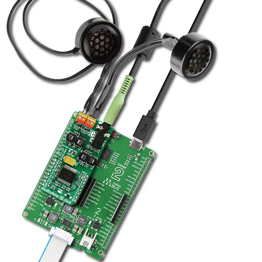
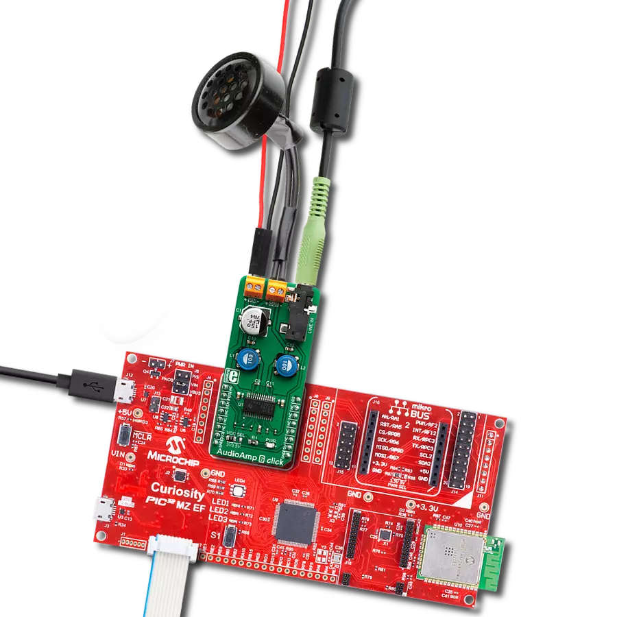
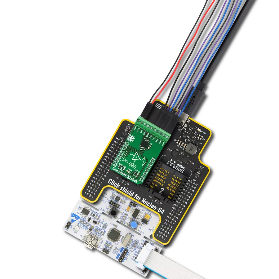
2x30W Amp Click
Dev. board
Clicker 2 for Kinetis
Compiler
NECTO Studio
MCU
MK64FN1M0VDC12
Whether you're a music enthusiast, a DIY audio project lover, or a professional sound designer, the 2x30W Amp Click is perfect for amplifying audio signals compactly and efficiently
A
A
Hardware Overview
How does it work?
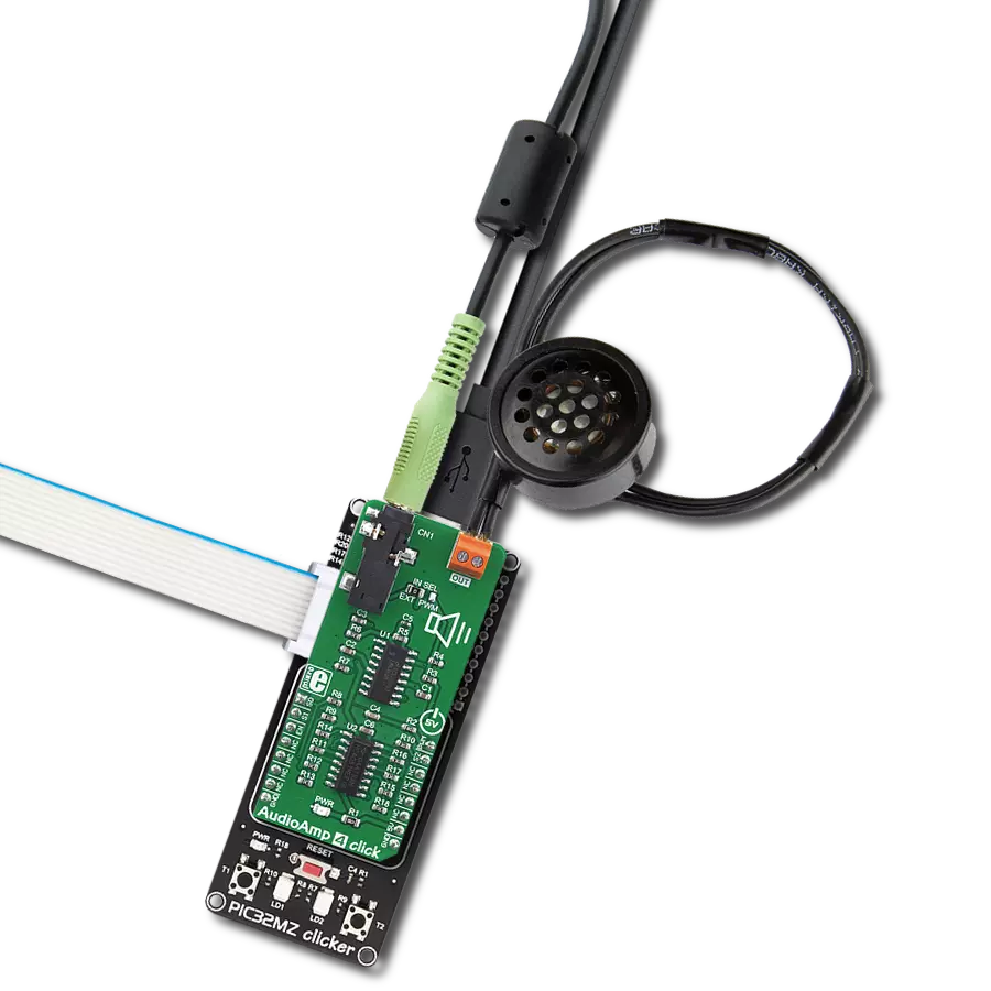
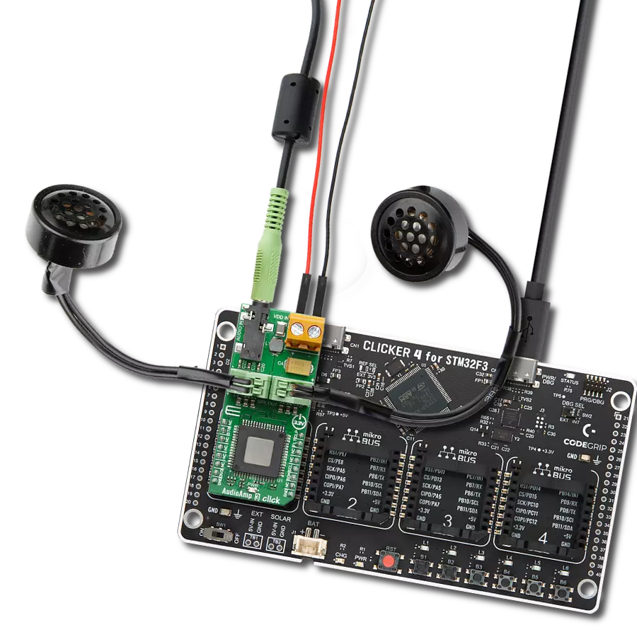
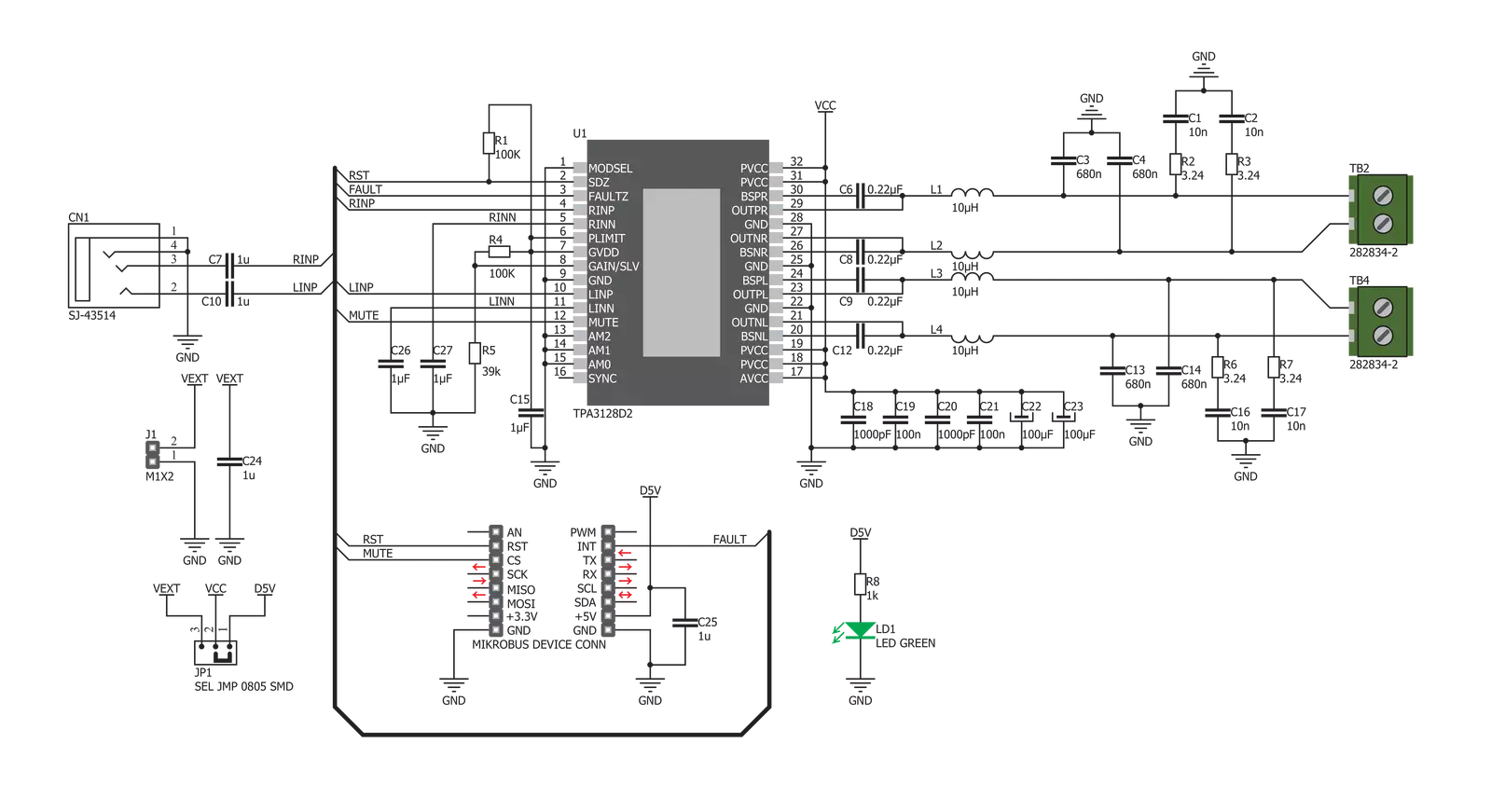
2x30W Amp Click is based on the TPA3128, 2x30-W class-D amplifier with low idle power dissipation from Texas Instruments. The most important characteristic of this IC is its output efficiency, which reduces the need for bulky heat sinks, usually associated with audio amplifiers. This is accomplished by switching MOSFET outputs, which have very low RDSON, as low as 90 mΩ. ClassD amplifiers are way more efficient by design than class A or AB amplifiers. Class D amplifier working principles are based on the switching characteristic of the transistors rather than the linear characteristic used for the A/AB class amplifiers. The audio signal is encoded into a PWM signal with a fixed amplitude. An output signal is restored through the LC filter and the speaker itself. Since the basis of this principle is switching the signal, and the transistors are either fully ON or fully OFF, they spend very little time in the linear region and dissipate very little power. Using low RDSON MOSFETs becomes possible and desirable so that the efficiency goes up to 90% and over. 2x30W Amp click is designed to work with two channels of a single-sided audio source, connected via the 3.5mm stereo audio jack provided on board. The Click board™ is equipped with a connector for the external power source.
By default, the 2x30 Amp click is supplied via the mikroBUS™ 5V rail, which limits the output power. An adequate external power supply should be used for the full output power. The TPA3128 IC can handle up to 26V. The onboard SMD jumper should be switched to the desired position (EXT or 5V) to select operation via the external power supply. If the EXT position is selected, the external power supply should be connected via the 1x2 header on the side of the Click board™, labeled as VEXT. The connected speaker impedance should not be less than 4Ω. The speakers can be connected via two edge connectors, with clearly labeled input ports: L+ and L- for connecting the left speaker's positive and negative terminals; R+ and R- for connecting the right speaker's positive and negative terminals. Care should be taken to dimension the speakers according to the maximum output power of the amplifier. The amplifier has a fixed gain of 32dB, determined by two resistors labeled R4 and R5 on the provided schematic. The RST pin of the mikroBUS™ is routed to the SDZ pin of the TPA3128 IC. Setting this pin to a LOW logic level will set the TPA3128 IC in the shutdown mode, with its output stage set to a high impedance (Hi-Z), reducing the idle current to a minimum.
Pulling the SDZ (RST) pin to a LOW logic level before disconnecting the power from the Click board™ to avoid audible power-off clicks is a good practice. The onboard resistor pulls the RST pin up to a HIGH logic level. Another way to mute the speakers is by pulling the MUTE pin to a HIGH logic level. This pin is routed to the CS pin of the mikroBUS™ and labeled as the MT. Pulling this pin to a HIGH logic level will also set the output stage to a Hi-Z, but it will perform a muting function only, thus muting the IC faster than the complete shutdown with the SDZ pin. This function is useful if used in conjunction with the FAULT pin, allowing power-up in a muted state when there is a problem on the output stage. The FAULTZ pin is routed to the INT pin of the mikroBUS™ and labeled as the FLT. It is used to signalize the fault condition (overtemperature, output DC offset detection) to the host MCU. It is active low and can trigger an interrupt request on the host MCU so that the proper action can be taken. The Click board™ uses only GPIO pins, which is extremely simple. However, the Click board™ comes equipped with a library containing easy-to-use functions and an example code that can be used, as a reference, for further development.

Features overview
Development board
Clicker 2 for Kinetis is a compact starter development board that brings the flexibility of add-on Click boards™ to your favorite microcontroller, making it a perfect starter kit for implementing your ideas. It comes with an onboard 32-bit ARM Cortex-M4F microcontroller, the MK64FN1M0VDC12 from NXP Semiconductors, two mikroBUS™ sockets for Click board™ connectivity, a USB connector, LED indicators, buttons, a JTAG programmer connector, and two 26-pin headers for interfacing with external electronics. Its compact design with clear and easily recognizable silkscreen markings allows you to build gadgets with unique functionalities and
features quickly. Each part of the Clicker 2 for Kinetis development kit contains the components necessary for the most efficient operation of the same board. In addition to the possibility of choosing the Clicker 2 for Kinetis programming method, using a USB HID mikroBootloader or an external mikroProg connector for Kinetis programmer, the Clicker 2 board also includes a clean and regulated power supply module for the development kit. It provides two ways of board-powering; through the USB Micro-B cable, where onboard voltage regulators provide the appropriate voltage levels to each component on the board, or
using a Li-Polymer battery via an onboard battery connector. All communication methods that mikroBUS™ itself supports are on this board, including the well-established mikroBUS™ socket, reset button, and several user-configurable buttons and LED indicators. Clicker 2 for Kinetis is an integral part of the Mikroe ecosystem, allowing you to create a new application in minutes. Natively supported by Mikroe software tools, it covers many aspects of prototyping thanks to a considerable number of different Click boards™ (over a thousand boards), the number of which is growing every day.

Microcontroller Overview
MCU Card / MCU

Architecture
ARM Cortex-M4
MCU Memory (KB)
1024
Silicon Vendor
NXP
Pin count
121
RAM (Bytes)
262144
Used MCU Pins
mikroBUS™ mapper
Take a closer look
Click board™ Schematic
Step by step
Project assembly

Start by selecting your development board and Click board™. Begin with the Clicker 2 for Kinetis as your development board.


Software Support
Library Description
This library contains API for 2x30W Amp Click driver.
Key functions:
c2x30wamp_enable- Device Enable functionc2x30wamp_mute- Device Mute functionc2x30wamp_check_diagnostic- Diagnostic Check function
Open Source
Code example
The complete application code and a ready-to-use project are available through the NECTO Studio Package Manager for direct installation in the NECTO Studio. The application code can also be found on the MIKROE GitHub account.
/*!
 * \file
 * \brief c2x30W Amp Click example
 *
 * # Description
 * This application is audio amplifier.
 *
 * The demo application is composed of two sections :
 *
 * ## Application Init
 * Initializes GPIO driver and enables the device.
 *
 * ## Application Task
 * Mute output for a period of 3 seconds, then keep it unmuted for a period of 10 seconds.
 * After that, checks if over current fault, over temperature fault or too high DC offset fault occurred.
 *
 * ## NOTE
 * When under or over voltage condition occurres the output goes to high impedance state,
 * but the FAULT pin will not be asserted.
 *
 * \author MikroE Team
 *
 */
// ------------------------------------------------------------------- INCLUDES

#include "board.h"
#include "log.h"
#include "c2x30wamp.h"

// ------------------------------------------------------------------ VARIABLES

static c2x30wamp_t c2x30wamp;
static log_t logger;

// ------------------------------------------------------ APPLICATION FUNCTIONS

void application_init ( void )
{
    log_cfg_t log_cfg;
    c2x30wamp_cfg_t cfg;

    /**
     * Logger initialization.
     * Default baud rate: 115200
     * Default log level: LOG_LEVEL_DEBUG
     * @note If USB_UART_RX and USB_UART_TX
     * are defined as HAL_PIN_NC, you will
     * need to define them manually for log to work.
     * See @b LOG_MAP_USB_UART macro definition for detailed explanation.
     */
    LOG_MAP_USB_UART( log_cfg );
    log_init( &logger, &log_cfg );
    log_info(&logger, "---- Application Init ----");

    //  Click initialization.

    c2x30wamp_cfg_setup( &cfg );
    C2X30WAMP_MAP_MIKROBUS( cfg, MIKROBUS_1 );
    c2x30wamp_init( &c2x30wamp, &cfg );

    c2x30wamp_enable( &c2x30wamp, C2X30WAMP_ENABLE );
    log_printf( &logger, "2x30W AMP is initialized \r\n" );
    Delay_ms ( 200 );
}

void application_task ( void )
{
    c2x30wamp_mute( &c2x30wamp, C2X30WAMP_MUTE );
    log_printf( &logger, "---------------------- \r\n" );
    log_printf( &logger, "MUTE \r\n" );
    Delay_ms ( 1000 );
    Delay_ms ( 1000 );
    Delay_ms ( 1000 );
    c2x30wamp_mute( &c2x30wamp, C2X30WAMP_UNMUTE );
    log_printf( &logger, "---------------------- \r\n" );
    log_printf( &logger, "UNMUTE \r\n" );
    // 10 seconds delay
    Delay_ms ( 1000 );
    Delay_ms ( 1000 );
    Delay_ms ( 1000 );
    Delay_ms ( 1000 );
    Delay_ms ( 1000 );
    Delay_ms ( 1000 );
    Delay_ms ( 1000 );
    Delay_ms ( 1000 );
    Delay_ms ( 1000 );
    Delay_ms ( 1000 );

    uint8_t fault_check = c2x30wamp_check_diagnostic( &c2x30wamp );

    if ( fault_check == 0 )
    {
        log_printf( &logger, "Fault condition! \r\n" );
    }
}

int main ( void )
{
    /* Do not remove this line or clock might not be set correctly. */
    #ifdef PREINIT_SUPPORTED
    preinit();
    #endif

    application_init( );

    for ( ; ; )
    {
        application_task( );
    }

    return 0;
}

// ------------------------------------------------------------------------ END
Additional Support
Resources
Category:Amplifier