Unlock precision with our programmable gain amplifier based on LTC6912 and PIC18F57Q43
Scale up your signals

Published Feb 13, 2024
Click board™
GainAMP Click
Dev. board
Curiosity Nano with PIC18F57Q43
Compiler
NECTO Studio
MCU
PIC18F57Q43
Our PGA solution enables seamless signal amplification with customizable gain settings, making it the ideal choice for your applications where precision and flexibility are paramount
A
A
Hardware Overview
How does it work?
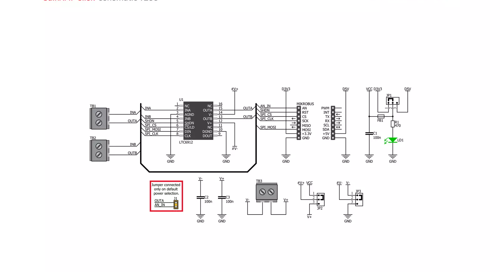
GainAMP Click is based on the LTC6912, a dual channel, low noise, digitally programmable gain amplifier (PGA) from Analog Devices. The click is designed to work on either a 3.3V or 5V power supply. It communicates with the target MCU over the SPI interface, with additional functionality provided by the following pins on the mikroBUS™ line: AN, RST. GainAMP Click also features three
screw terminals and a power indication LED. The gains for both channels are independently programmable, using a 3-wire SPI interface to select voltage gains of 0, 1, 2, 5, 10, 20, 50, and 100V/V (LTC6912-1). All gains are inverting. The LTC6912 consists of 2 matched amplifiers with rail-to-rail outputs. When operated with unity gain, they will also process rail-to-rail input signals.
A half-supply reference generated internally at the AGND pin supports single power supply applications. It operates from single or split supplies from 2.7V to 10.5V in total. A programmable-gain amplifier (PGA) is an electronic amplifier whose gain can be controlled externally (by analog or digital signals).

Features overview
Development board
PIC18F57Q43 Curiosity Nano evaluation kit is a cutting-edge hardware platform designed to evaluate microcontrollers within the PIC18-Q43 family. Central to its design is the inclusion of the powerful PIC18F57Q43 microcontroller (MCU), offering advanced functionalities and robust performance. Key features of this evaluation kit include a yellow user LED and a responsive
mechanical user switch, providing seamless interaction and testing. The provision for a 32.768kHz crystal footprint ensures precision timing capabilities. With an onboard debugger boasting a green power and status LED, programming and debugging become intuitive and efficient. Further enhancing its utility is the Virtual serial port (CDC) and a debug GPIO channel (DGI
GPIO), offering extensive connectivity options. Powered via USB, this kit boasts an adjustable target voltage feature facilitated by the MIC5353 LDO regulator, ensuring stable operation with an output voltage ranging from 1.8V to 5.1V, with a maximum output current of 500mA, subject to ambient temperature and voltage constraints.

Microcontroller Overview
MCU Card / MCU

Architecture
PIC
MCU Memory (KB)
128
Silicon Vendor
Microchip
Pin count
48
RAM (Bytes)
8196
You complete me!
Accessories
Curiosity Nano Base for Click boards is a versatile hardware extension platform created to streamline the integration between Curiosity Nano kits and extension boards, tailored explicitly for the mikroBUS™-standardized Click boards and Xplained Pro extension boards. This innovative base board (shield) offers seamless connectivity and expansion possibilities, simplifying experimentation and development. Key features include USB power compatibility from the Curiosity Nano kit, alongside an alternative external power input option for enhanced flexibility. The onboard Li-Ion/LiPo charger and management circuit ensure smooth operation for battery-powered applications, simplifying usage and management. Moreover, the base incorporates a fixed 3.3V PSU dedicated to target and mikroBUS™ power rails, alongside a fixed 5.0V boost converter catering to 5V power rails of mikroBUS™ sockets, providing stable power delivery for various connected devices.

Used MCU Pins
mikroBUS™ mapper
Take a closer look
Click board™ Schematic
Step by step
Project assembly

Start by selecting your development board and Click board™. Begin with the Curiosity Nano with PIC18F57Q43 as your development board.


Track your results in real time
Application Output
1. Application Output - In Debug mode, the 'Application Output' window enables real-time data monitoring, offering direct insight into execution results. Ensure proper data display by configuring the environment correctly using the provided tutorial.

2. UART Terminal - Use the UART Terminal to monitor data transmission via a USB to UART converter, allowing direct communication between the Click board™ and your development system. Configure the baud rate and other serial settings according to your project's requirements to ensure proper functionality. For step-by-step setup instructions, refer to the provided tutorial.

3. Plot Output - The Plot feature offers a powerful way to visualize real-time sensor data, enabling trend analysis, debugging, and comparison of multiple data points. To set it up correctly, follow the provided tutorial, which includes a step-by-step example of using the Plot feature to display Click board™ readings. To use the Plot feature in your code, use the function: plot(*insert_graph_name*, variable_name);. This is a general format, and it is up to the user to replace 'insert_graph_name' with the actual graph name and 'variable_name' with the parameter to be displayed.

Software Support
Library Description
This library contains API for GainAMP Click driver.
Key functions:
gainamp_read_an_pin_value- GainAMP read AN pin value functiongainamp_read_an_pin_voltage- GainAMP read AN pin voltage level functiongainamp_set_gain- Function for sets gain of the GainAMP Click
Open Source
Code example
The complete application code and a ready-to-use project are available through the NECTO Studio Package Manager for direct installation in the NECTO Studio. The application code can also be found on the MIKROE GitHub account.
/*!
 * @file main.c
 * @brief GainAMP Click example
 *
 * # Description
 * This is an example that demonstrates the use of the GainAMP Click board.
 *
 * The demo application is composed of two sections :
 *
 * ## Application Init
 * Initializes SPI module and set CS pin and RST pin as OUTPUT,
 * initialization driver init and resets chip.
 *
 * ## Application Task
 * Sets the gain for both channels, channel A and channel B.
 *
 * @author Stefan Ilic
 *
 */

#include "board.h"
#include "log.h"
#include "gainamp.h"

static gainamp_t gainamp;
static log_t logger;

void application_init ( void )
{
    log_cfg_t log_cfg;  /**< Logger config object. */
    gainamp_cfg_t gainamp_cfg;  /**< Click config object. */

    /**
     * Logger initialization.
     * Default baud rate: 115200
     * Default log level: LOG_LEVEL_DEBUG
     * @note If USB_UART_RX and USB_UART_TX
     * are defined as HAL_PIN_NC, you will
     * need to define them manually for log to work.
     * See @b LOG_MAP_USB_UART macro definition for detailed explanation.
     */
    LOG_MAP_USB_UART( log_cfg );
    log_init( &logger, &log_cfg );
    log_info( &logger, " Application Init " );

    // Click initialization.

    gainamp_cfg_setup( &gainamp_cfg );
    GAINAMP_MAP_MIKROBUS( gainamp_cfg, MIKROBUS_1 );
    err_t init_flag  = gainamp_init( &gainamp, &gainamp_cfg );
    if ( ( SPI_MASTER_ERROR == init_flag ) || ( ADC_ERROR == init_flag ) ) {
        log_error( &logger, " Application Init Error. " );
        log_info( &logger, " Please, run program again... " );

        for ( ; ; );
    }
    gainamp_reset( &gainamp );
    Delay_ms ( 100 );

    log_info( &logger, " Application Task " );
}

void application_task ( void )
{
    gainamp_set_gain( &gainamp, GAINAMP_CHANNEL_A_x1 | GAINAMP_CHANNEL_B_x5 );
    // 10 seconds delay
    Delay_ms ( 1000 );
    Delay_ms ( 1000 );
    Delay_ms ( 1000 );
    Delay_ms ( 1000 );
    Delay_ms ( 1000 );
    Delay_ms ( 1000 );
    Delay_ms ( 1000 );
    Delay_ms ( 1000 );
    Delay_ms ( 1000 );
    Delay_ms ( 1000 );

    gainamp_set_gain( &gainamp, GAINAMP_CHANNEL_A_x10 | GAINAMP_CHANNEL_B_x100 );
    // 10 seconds delay
    Delay_ms ( 1000 );
    Delay_ms ( 1000 );
    Delay_ms ( 1000 );
    Delay_ms ( 1000 );
    Delay_ms ( 1000 );
    Delay_ms ( 1000 );
    Delay_ms ( 1000 );
    Delay_ms ( 1000 );
    Delay_ms ( 1000 );
    Delay_ms ( 1000 );
}

int main ( void )
{
    /* Do not remove this line or clock might not be set correctly. */
    #ifdef PREINIT_SUPPORTED
    preinit();
    #endif

    application_init( );

    for ( ; ; )
    {
        application_task( );
    }

    return 0;
}

// ------------------------------------------------------------------------ END
Additional Support
Resources
Category:Amplifier