Perform step-down conversion of the applied DC input with MAX17536 and PIC18F57Q43
Transform voltage with ease

Published Jul 31, 2023
Click board™
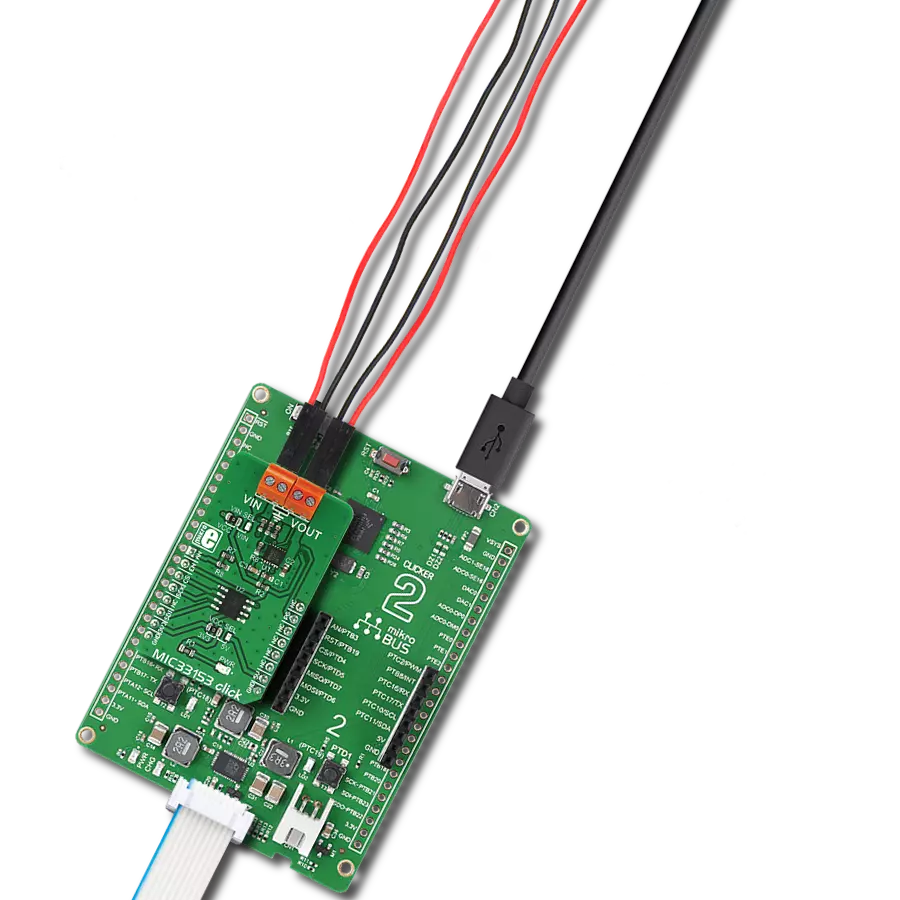
Buck 8 Click
Dev. board
UNI Clicker
Compiler
NECTO Studio
MCU
PIC18F57Q43
Experience stable and reliable voltage output with this embedded solution!
A
A
Hardware Overview
How does it work?
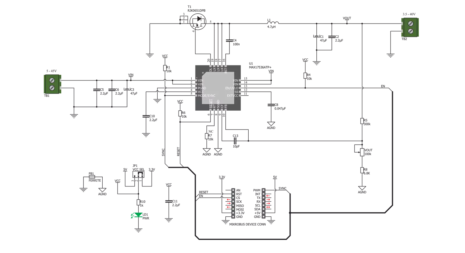
Buck 8 Click is based on the MAX17536, a high-efficiency, synchronous step-down DC-DC converter with internal compensation from Analog Devices. The MAX17536 is an advanced integrated step-down converter that can deliver a reasonably high current up to 4A. The input voltage can range between 5V and 45V. It should stay about 10% above the desired output voltage. This means that the output voltage ranges from 0.9V to 0.9 x Vin, where Vin is the input voltage. A precise multi-turn potentiometer can adjust the output voltage. This potentiometer allows adjustment of the output voltage level by changing the resistance value of the voltage divider that feeds part of the output voltage back to the FB pin of the MAX17536. Since the potentiometer is a mechanical component, it will allow the output voltage to remain the same, even after the power cycle. Although it can deliver up to 4A, the output current is limited by the maximum power dissipation of the converter. Although the percentage of the power lost on dissipation varies with both input voltage and output current, it can be assumed that this power loss is 10%. According to the datasheet, the maximum advisable power dissipation is 2.67W. To allow for some overhead, assuming that the maximum power dissipation is 2W is safe. This means that the maximum output power is about 20W. The MAX17536 features robust overload and short-circuit protection. When the internally set current limit of 6.5A is exceeded, the high-side MOSFET is turned off, and the hiccup mode is triggered. This mode suspends the
operation for 32,768 duty cycles, after which the soft start sequence is reattempted. If the fault condition is present at the startup and the output voltage remains under 68% of the nominal value, the hiccup mode is also activated. The thermal protection ensures that the junction temperature of the IC stays below 165˚C. The device shuts down when this temperature is exceeded, allowing it to cool down. When the junction temperature drops to about 10˚C, the device is restarted. The output voltage condition can be monitored via the #RESET pin of the MAX17536. This pin is an open drain output, and it is pulled to a HIGH logic level by the onboard resistor. It is routed to the RST pin of the mikroBUS™ and can be used as the power good indication. This pin is driven to a LOW logic level when the output voltage drops below 92.2% of the nominal regulated output voltage. The #RESET pin also reports a thermal shutdown event. The soft start feature prevents the inrush current. The soft start capacitor determines this feature. The soft start is set to about 18ms by the 100nF capacitor. The SYNC/MODE pin is pulled to a high logic level, allowing the device to work in the DCM light load mode, allowing more efficient operation when the light load is connected to the output. By driving the MODE/SYNC pin to a LOW logic level, the device is forced into the PWM mode, which allows the least noise and ripple on the output, but it is not that efficient when working with light loads. The MODE/SYNC pin is routed to the PWM pin of the mikroBUS™ and pulled to a HIGH logic level by the
onboard pull-up resistor. The device latches the state of this pin at the startup, ignoring pin state changes after the startup sequence is finished. One of the distinctive features of this buck converter is the ability to synchronize the switching clock frequency with an external clock signal. It is possible to synchronize the switching frequency within a range of about 1.1 to 1.4 higher than the value set on the Buck 8 Click, which is 450kHz. This feature primarily synchronizes switching frequencies when more than one buck converter is used. When the valid synchronization signal is applied to the MODE/SYNC pin, the device will switch to the PWM mode, with the switching frequency synchronized with the input signal. In this case, after the synchronization signal is disconnected, the device will remain working in the PWM mode. The EN pin of the MAX17572 is routed to the CS pin of the mikroBUS™. This pin enables the buck converter when driven to a HIGH logic level, but it can also be used to set the Undervoltage lockout threshold. If the input voltage falls under this threshold, the internal low drop output regulators (LDOs) will not power on the internal logic, and the buck converter will stay disabled. The Buck 8 Click features an SMD jumper, which sets the logical voltage levels for the pins, allowing both 3.3V and 5V MCUs to be used with the Click board™. The board is also equipped with input and output screw terminals, which allow a secure connection between the input voltage source and the load.

Features overview
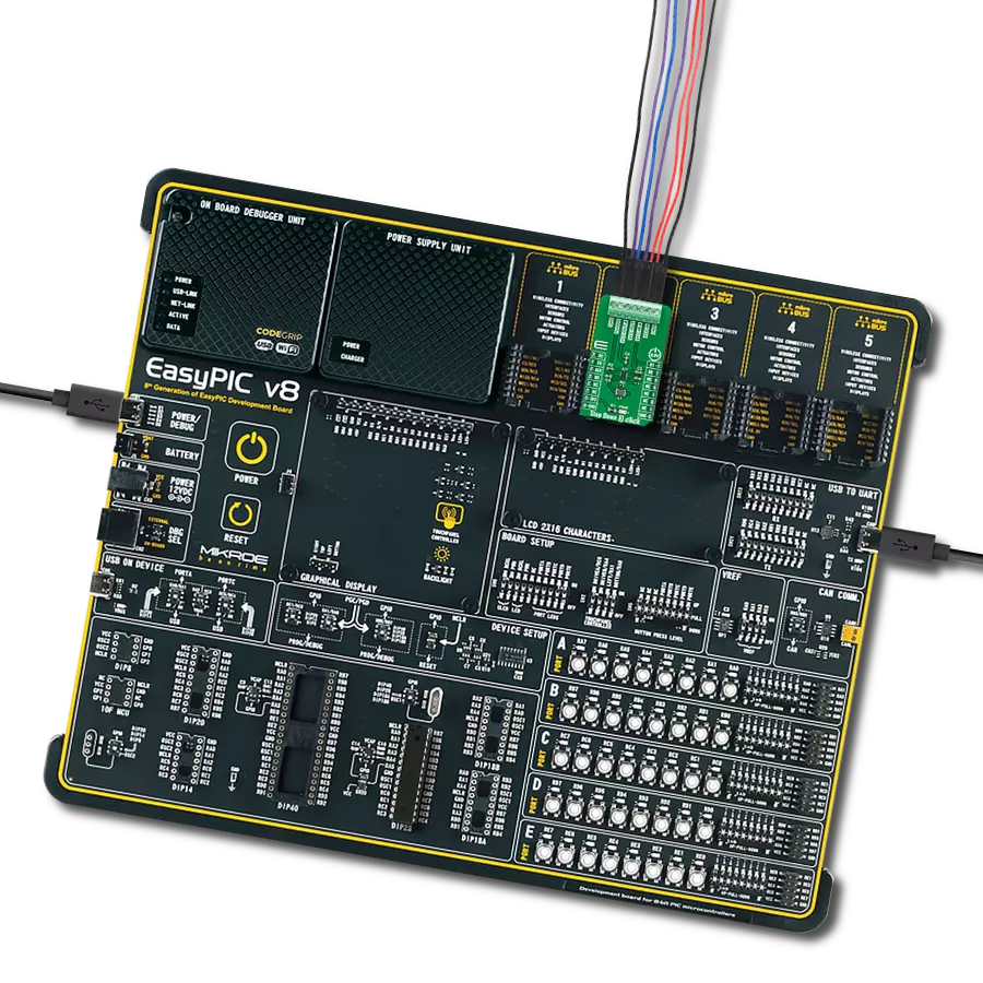
Development board
UNI Clicker is a compact development board designed as a complete solution that brings the flexibility of add-on Click boards™ to your favorite microcontroller, making it a perfect starter kit for implementing your ideas. It supports a wide range of microcontrollers, such as different ARM, PIC32, dsPIC, PIC, and AVR from various vendors like Microchip, ST, NXP, and TI (regardless of their number of pins), four mikroBUS™ sockets for Click board™ connectivity, a USB connector, LED indicators, buttons, a debugger/programmer connector, and two 26-pin headers for interfacing with external electronics. Thanks to innovative manufacturing technology, it allows you to build
gadgets with unique functionalities and features quickly. Each part of the UNI Clicker development kit contains the components necessary for the most efficient operation of the same board. In addition to the possibility of choosing the UNI Clicker programming method, using a third-party programmer or CODEGRIP/mikroProg connected to onboard JTAG/SWD header, the UNI Clicker board also includes a clean and regulated power supply module for the development kit. It provides two ways of board-powering; through the USB Type-C (USB-C) connector, where onboard voltage regulators provide the appropriate voltage levels to each component on the board, or using a Li-Po/Li
Ion battery via an onboard battery connector. All communication methods that mikroBUS™ itself supports are on this board (plus USB HOST/DEVICE), including the well-established mikroBUS™ socket, a standardized socket for the MCU card (SiBRAIN standard), and several user-configurable buttons and LED indicators. UNI Clicker is an integral part of the Mikroe ecosystem, allowing you to create a new application in minutes. Natively supported by Mikroe software tools, it covers many aspects of prototyping thanks to a considerable number of different Click boards™ (over a thousand boards), the number of which is growing every day.

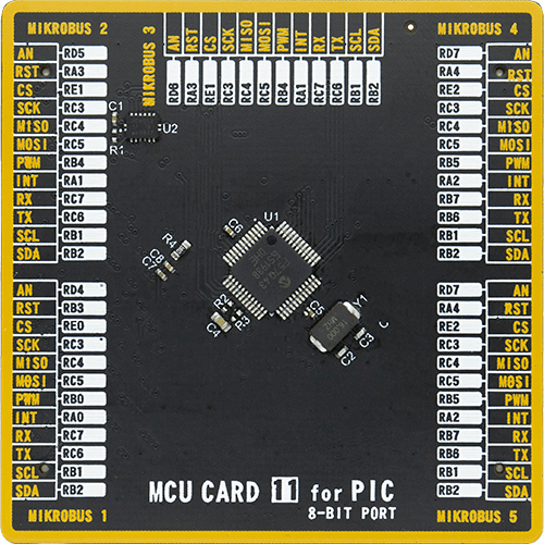
Microcontroller Overview
MCU Card / MCU
Type
8th Generation
Architecture
PIC
MCU Memory (KB)
128
Silicon Vendor
Microchip
Pin count
48
RAM (Bytes)
8196
Used MCU Pins
mikroBUS™ mapper
Take a closer look
Click board™ Schematic
Step by step
Project assembly

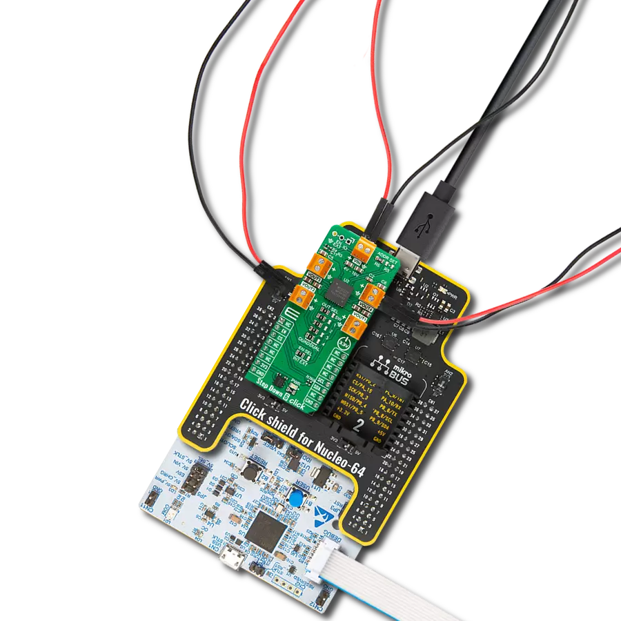
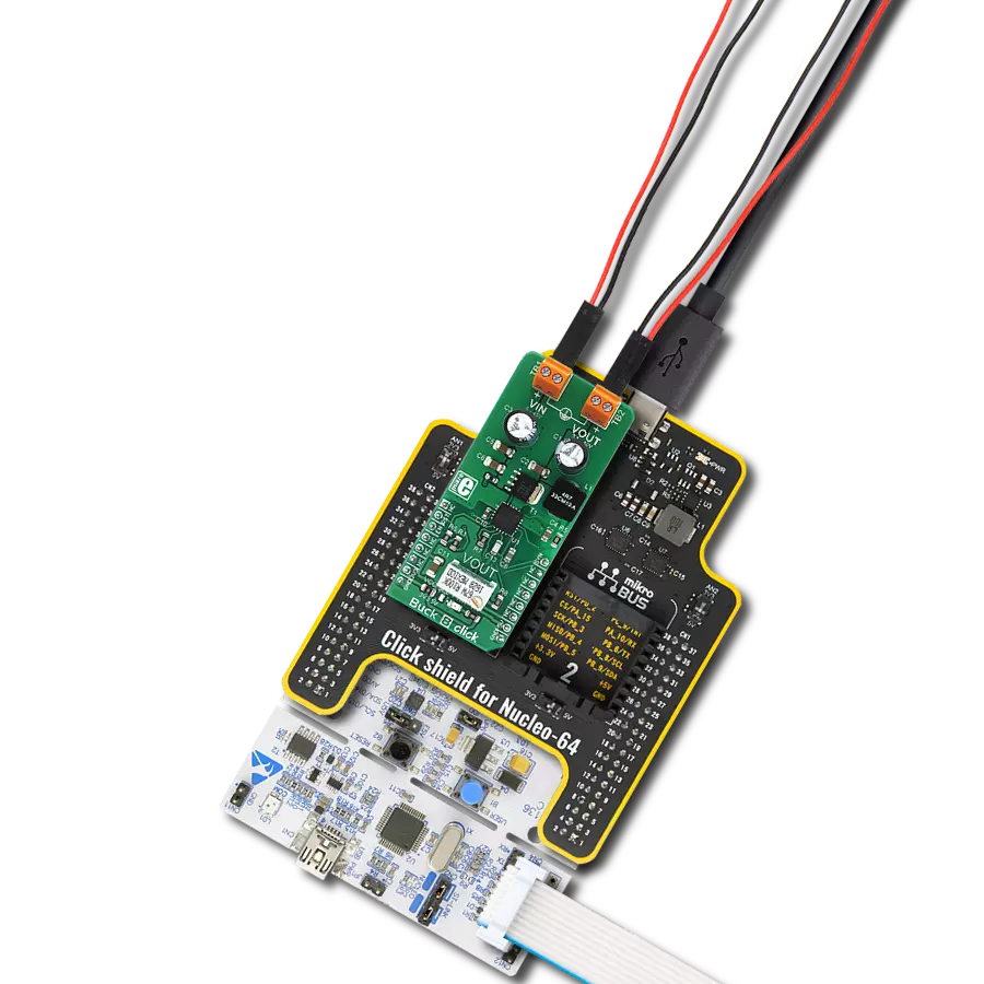
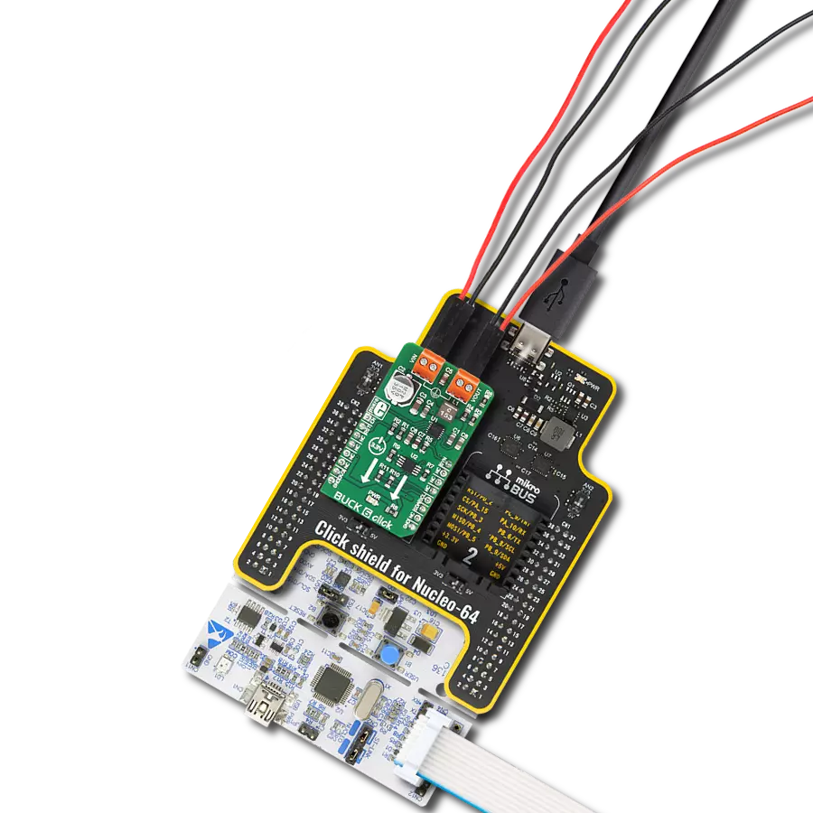
Start by selecting your development board and Click board™. Begin with the UNI Clicker as your development board.


Track your results in real time
Application Output
1. Application Output - In Debug mode, the 'Application Output' window enables real-time data monitoring, offering direct insight into execution results. Ensure proper data display by configuring the environment correctly using the provided tutorial.

2. UART Terminal - Use the UART Terminal to monitor data transmission via a USB to UART converter, allowing direct communication between the Click board™ and your development system. Configure the baud rate and other serial settings according to your project's requirements to ensure proper functionality. For step-by-step setup instructions, refer to the provided tutorial.

3. Plot Output - The Plot feature offers a powerful way to visualize real-time sensor data, enabling trend analysis, debugging, and comparison of multiple data points. To set it up correctly, follow the provided tutorial, which includes a step-by-step example of using the Plot feature to display Click board™ readings. To use the Plot feature in your code, use the function: plot(*insert_graph_name*, variable_name);. This is a general format, and it is up to the user to replace 'insert_graph_name' with the actual graph name and 'variable_name' with the parameter to be displayed.

Software Support
Library Description
This library contains API for Buck 8 Click driver.
Key functions:
buck8_get_state- Get state of pinbuck8_set_power_mode- Function settings mode
Open Source
Code example
The complete application code and a ready-to-use project are available through the NECTO Studio Package Manager for direct installation in the NECTO Studio. The application code can also be found on the MIKROE GitHub account.
/*!
 * \file
 * \brief Buck 8 Click example
 *
 * # Description
 * Demo application shows basic usage of BUCK 8 Clicks.
 *
 * The demo application is composed of two sections :
 *
 * ## Application Init
 * Configures the driver and enables the Click board.
 *
 * ## Application Task
 * Reads the VOUT state and parses it on USB UART.
 *
 * \author Katarina Perendic
 *
 */
// ------------------------------------------------------------------- INCLUDES

#include "board.h"
#include "log.h"
#include "buck8.h"

// ------------------------------------------------------------------ VARIABLES

static buck8_t buck8;
static log_t logger;

// ------------------------------------------------------ APPLICATION FUNCTIONS

void application_init ( void )
{
    log_cfg_t log_cfg;
    buck8_cfg_t cfg;

    /**
     * Logger initialization.
     * Default baud rate: 115200
     * Default log level: LOG_LEVEL_DEBUG
     * @note If USB_UART_RX and USB_UART_TX
     * are defined as HAL_PIN_NC, you will
     * need to define them manually for log to work.
     * See @b LOG_MAP_USB_UART macro definition for detailed explanation.
     */
    LOG_MAP_USB_UART( log_cfg );
    log_init( &logger, &log_cfg );
    log_info( &logger, "---- Application Init ----" );

    //  Click initialization.

    buck8_cfg_setup( &cfg );
    BUCK8_MAP_MIKROBUS( cfg, MIKROBUS_1 );
    buck8_init( &buck8, &cfg );

    buck8_default_cfg( &buck8 );
}

void application_task ( void )
{
    uint8_t pg_state;

    pg_state = buck8_get_state( &buck8 );

    if ( pg_state == 1 )
    {
        log_info( &logger, "VOUT is below 92.2%% of VIN" );
    }
    else
    {
        log_info( &logger, "VOUT is above 92.2%% of VIN" );
    }

    Delay_1sec();
}

int main ( void )
{
    /* Do not remove this line or clock might not be set correctly. */
    #ifdef PREINIT_SUPPORTED
    preinit();
    #endif

    application_init( );

    for ( ; ; )
    {
        application_task( );
    }

    return 0;
}


// ------------------------------------------------------------------------ END