Create the ultimate solution for signal magnification with MCP6S21 and PIC32MX695F512L
Amplify with precision

Published Jun 08, 2023
Click board™
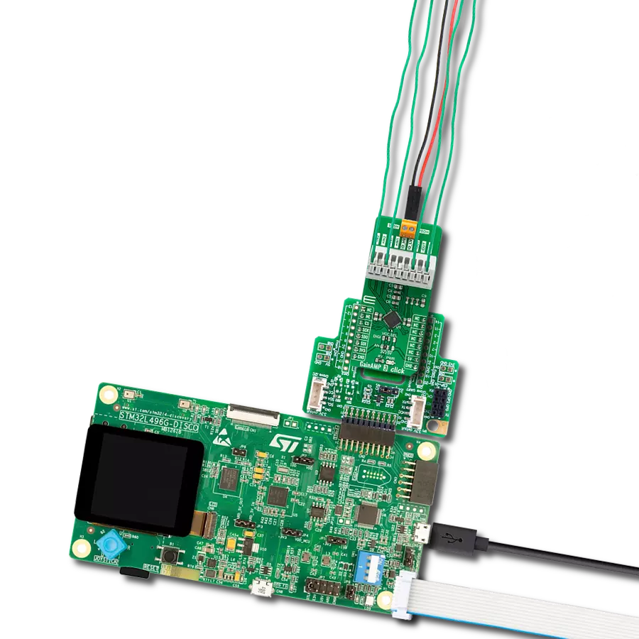
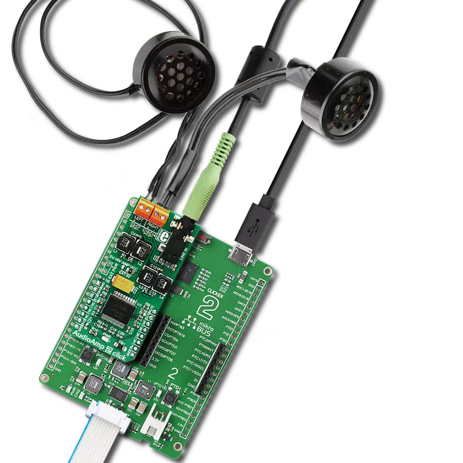
GainAMP 2 click
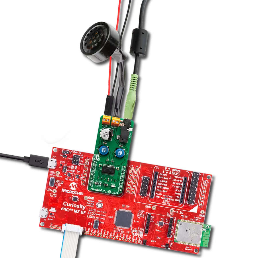
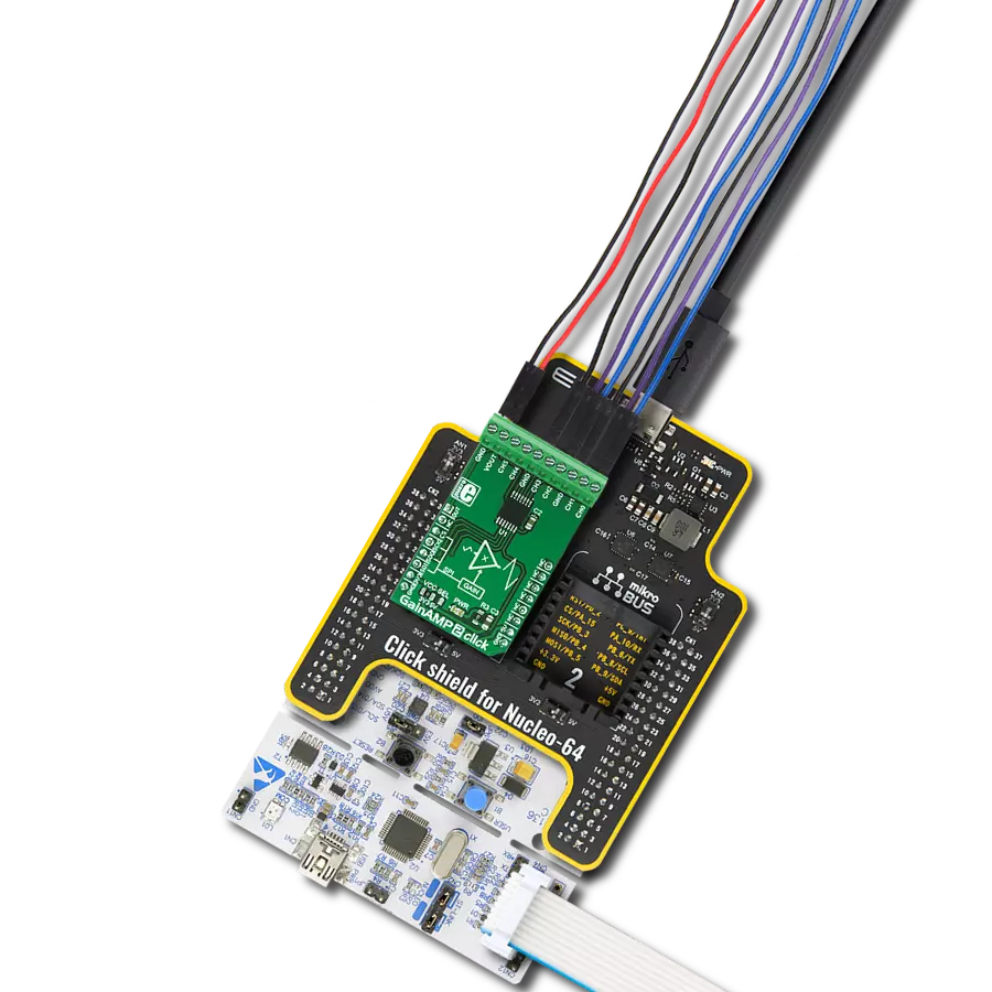
Dev. board
UNI Clicker
Compiler
NECTO Studio
MCU
PIC32MX695F512L
Whether you're working with audio, sensor data, or other low-level signals, our 6-channel programmable gain amplifier is an ideal solution for boosting and optimizing signal quality
A
A
Hardware Overview
How does it work?
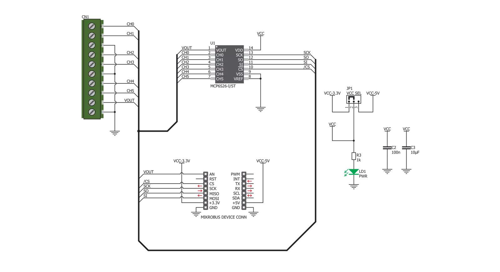
GainAMP 2 Click is based on the MCP6S21, a rail-to-rail I/O, low noise programmable gain amplifier (PGA) from Microchip. This integrated circuit features six multiplexed non-inverting inputs, with a gain that can be programmed via the SPI interface for each input individually. The channels CH0 to CH5 are the six input channels connected to the external signal sources. The internal multiplexer selects the channel that is gained and sent to the output pin. The gain stage of the MCP6S21 has eight different discrete steps of gain: 1, 2, 4, 5, 8, 10, 16, and 32V/V. The rail-to-rail inputs and outputs accept voltage levels up to VCC with no distortions or phase shifting. The output voltage is offset by the resistor ladder network on
the output stage and the voltage on the voltage reference pin. Besides the VOUT pin on the ten-pole I/O connector, the MCP6S21 output pin is also routed to the AN pin of the mikroBUS™ so it can be used as the input signal for the ADC. This allows the amplified signal to be easily digitalized and processed by the MCU. Using the click board in this configuration effectively turns the GainAMP 2 click into an analog port expander with the selectable gain on its inputs. The MCP6S21 device can be put in a shutdown mode by setting the appropriate bits of the internal register via the SPI interface. While in shutdown mode, the power consumption is minimal. The device stays in Shutdown mode until a valid command is received
via the SPI. While in the shutdown mode, the device remembers the states of the internal registers, so when it awakens, it will resume working as before. The internal registers can be easily accessed by using MIKROE library functions. More information about the registers and their settings can be found in the MCP6S21 datasheet. This Click board™ can operate with either 3.3V or 5V logic voltage levels selected via the VCC SEL jumper. This way, both 3.3V and 5V capable MCUs can use the communication lines properly. However, the Click board™ comes equipped with a library containing easy-to-use functions and an example code that can be used, as a reference, for further development.

Features overview
Development board
UNI Clicker is a compact development board designed as a complete solution that brings the flexibility of add-on Click boards™ to your favorite microcontroller, making it a perfect starter kit for implementing your ideas. It supports a wide range of microcontrollers, such as different ARM, PIC32, dsPIC, PIC, and AVR from various vendors like Microchip, ST, NXP, and TI (regardless of their number of pins), four mikroBUS™ sockets for Click board™ connectivity, a USB connector, LED indicators, buttons, a debugger/programmer connector, and two 26-pin headers for interfacing with external electronics. Thanks to innovative manufacturing technology, it allows you to build
gadgets with unique functionalities and features quickly. Each part of the UNI Clicker development kit contains the components necessary for the most efficient operation of the same board. In addition to the possibility of choosing the UNI Clicker programming method, using a third-party programmer or CODEGRIP/mikroProg connected to onboard JTAG/SWD header, the UNI Clicker board also includes a clean and regulated power supply module for the development kit. It provides two ways of board-powering; through the USB Type-C (USB-C) connector, where onboard voltage regulators provide the appropriate voltage levels to each component on the board, or using a Li-Po/Li
Ion battery via an onboard battery connector. All communication methods that mikroBUS™ itself supports are on this board (plus USB HOST/DEVICE), including the well-established mikroBUS™ socket, a standardized socket for the MCU card (SiBRAIN standard), and several user-configurable buttons and LED indicators. UNI Clicker is an integral part of the Mikroe ecosystem, allowing you to create a new application in minutes. Natively supported by Mikroe software tools, it covers many aspects of prototyping thanks to a considerable number of different Click boards™ (over a thousand boards), the number of which is growing every day.

Microcontroller Overview
MCU Card / MCU
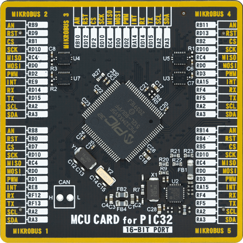
Type
8th Generation
Architecture
PIC32
MCU Memory (KB)
512
Silicon Vendor
Microchip
Pin count
100
RAM (Bytes)
131072
Used MCU Pins
mikroBUS™ mapper
Take a closer look
Click board™ Schematic
Step by step
Project assembly

Start by selecting your development board and Click board™. Begin with the UNI Clicker as your development board.


Software Support
Library Description
This library contains API for GainAMP 2 Click driver.
Key functions:
gainamp2_set_channel_gain- Set the channel gaingainamp2_get_voltage- Return voltage measured from VOUT pingainamp2_write_Command- Send Command
Open Source
Code example
The complete application code and a ready-to-use project are available through the NECTO Studio Package Manager for direct installation in the NECTO Studio. The application code can also be found on the MIKROE GitHub account.
/*!
 * \file
 * \brief GainAmp2 Click example
 *
 * # Description
 * This application is programmable gain amplifier
 *
 * The demo application is composed of two sections :
 *
 * ## Application Init
 * Initializes and sets GainAMP 2 Click channel 0 to amplify the signal 2 times
 *
 * ## Application Task
 * Displays the voltage measured from VOUT pin
 *
 * \author MikroE Team
 *
 */
// ------------------------------------------------------------------- INCLUDES

#include "board.h"
#include "log.h"
#include "gainamp2.h"

// ------------------------------------------------------------------ VARIABLES

static gainamp2_t gainamp2;
static log_t logger;

// ------------------------------------------------------ APPLICATION FUNCTIONS

void application_init ( void )
{
    log_cfg_t log_cfg;
    gainamp2_cfg_t cfg;

    /**
     * Logger initialization.
     * Default baud rate: 115200
     * Default log level: LOG_LEVEL_DEBUG
     * @note If USB_UART_RX and USB_UART_TX
     * are defined as HAL_PIN_NC, you will
     * need to define them manually for log to work.
     * See @b LOG_MAP_USB_UART macro definition for detailed explanation.
     */
    LOG_MAP_USB_UART( log_cfg );
    log_init( &logger, &log_cfg );
    log_info( &logger, "---- Application Init ----" );

    //  Click initialization.

    gainamp2_cfg_setup( &cfg );
    GAINAMP2_MAP_MIKROBUS( cfg, MIKROBUS_1 );
    gainamp2_init( &gainamp2, &cfg );

    gainamp2_set_channel_gain ( &gainamp2, GAINAMP2_CH0, GAINAMP2_GAIN_2X );
    log_printf( &logger,"Channel 0 - aplified 2x \r\n" );
}

void application_task( void )
{
    log_printf( &logger,"Voltage at VOUT: %f \r\n", gainamp2_get_voltage( &gainamp2 ) );
    log_printf( &logger,"------------------------------- \r\n " );
    Delay_ms ( 1000 );
}

int main ( void )
{
    /* Do not remove this line or clock might not be set correctly. */
    #ifdef PREINIT_SUPPORTED
    preinit();
    #endif

    application_init( );

    for ( ; ; )
    {
        application_task( );
    }

    return 0;
}

// ------------------------------------------------------------------------ END