Harness the power of a high-speed CAN transceiver with TLE9251V and PIC18F45K40
CANquer challenges
Published Nov 01, 2023
Click board™
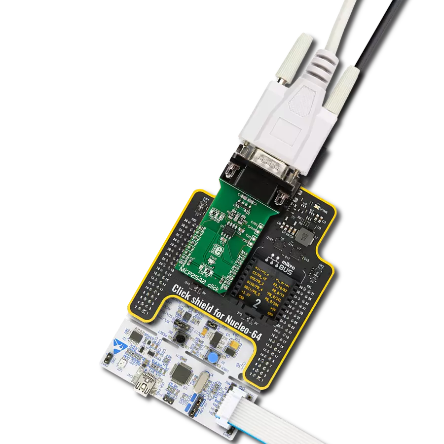
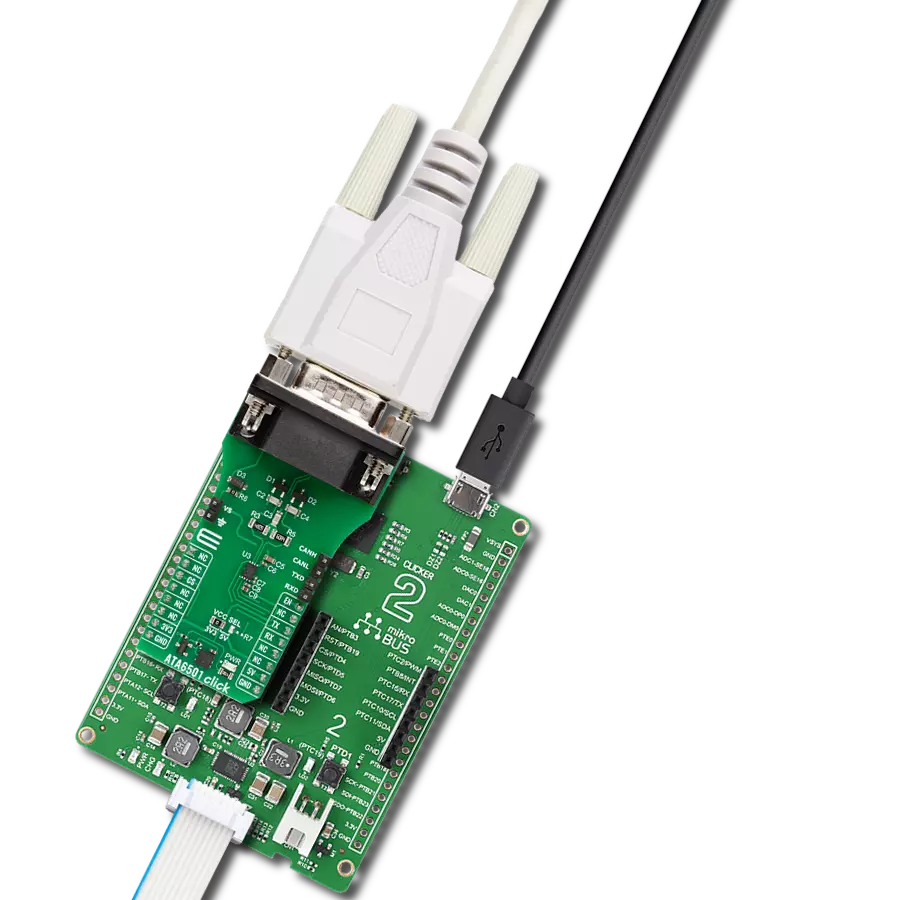
CAN FD 3 Click
Dev. board
Curiosity HPC
Compiler
NECTO Studio
MCU
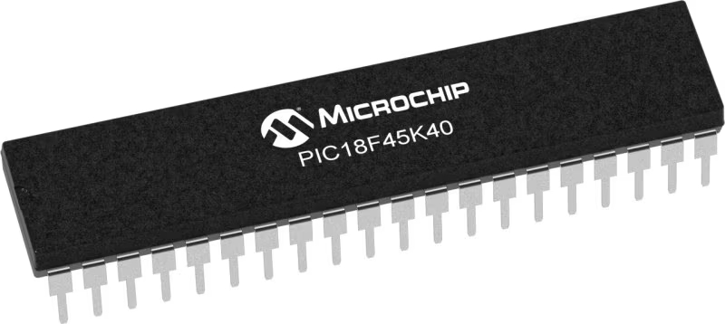
PIC18F45K40
Maximize data throughput with our high-speed CAN FD transceiver, ensuring seamless communication in the automotive industry
A
A
Hardware Overview
How does it work?
CAN FD 3 Click is based on the TLE9251V, a High-Speed CAN transceiver operating as an interface between the CAN controller and the physical bus medium from Infineon. An HS CAN network is a two-wire, differential network that allows data transmission rates up to 5 MBit/s. The characteristic of an HS CAN network is the two signal states on the CAN bus: dominant and recessive. The CANH and CANL pins are the interface to the CAN bus and operate as input and output. The RxD and TxD pins are the interface to the microcontroller. The TxD pin is the serial data input from the CAN controller. The RxD pin is the serial data output to the CAN controller. The HS CAN transceiver TLE9251V includes a receiver and a transmitter unit, allowing the transceiver to send data to the bus medium and monitor the data from the bus medium simultaneously. The HS CAN transceiver TLE9251V converts the serial data stream, available on the transmit data input TxD, into a differential output signal on the CAN bus
provided by the CANH and CANL pins. The receiver stage of the TLE9251V monitors the data on the CAN bus and converts it to a serial, single-ended signal on the RxD output pin. A logical "low" signal on the TxD pin creates a dominant signal on the CAN bus, followed by a logical "low" signal on the RxD pin. The feature broadcasting data to the CAN bus and listening to the data traffic on the CAN bus simultaneously is essential to support the bit-to-bit arbitration within CAN networks. Based on the high symmetry of the CANH and CANL output signals, the TLE9251V provides a low level of electromagnetic emission (EME) within a wide frequency range. The TLE9251V fulfills even stringent EMC test limits without additional external circuits, like a common mode choke. In Power On Reset, all functions of the TLE9251V are disabled, and the device is switched off. The TLE9251V has an integrated overtemperature detection to protect the TLE9251V against the thermal overstress of the transmitter. The
overtemperature protection is active in Normal-operating Mode and is disabled in all other Modes. The temperature sensor provides one temperature threshold: TJSD.When the temperature exceeds the threshold, TJSD the transmitter is disabled. This overtemperature event will be signaled as logical "low" on the ERR output pin in Normal-operating Mode. After the device has cooled down, the transmitter is re-enabled, and NERR returns to logical "high." Hysteresis is implemented within the temperature sensor. Given all its components' features, the CAN FD Click is best used for infotainment applications, cluster modules, radar applications, and HVAC. The onboard SMD jumper labeled the VIO SEL selects which voltage rail will be used as the logic voltage level. It offers voltage selection between 3.3V and 5V so that the click board™ can be interfaced with both the 3.3V and 5V capable MCUs. The two UART wires (RX and TX) can also be connected directly through two pins on the board's left edge.

Features overview
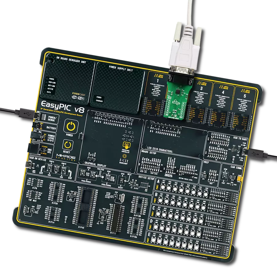
Development board
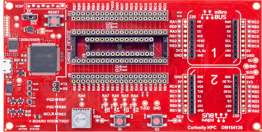
Curiosity HPC, standing for Curiosity High Pin Count (HPC) development board, supports 28- and 40-pin 8-bit PIC MCUs specially designed by Microchip for the needs of rapid development of embedded applications. This board has two unique PDIP sockets, surrounded by dual-row expansion headers, allowing connectivity to all pins on the populated PIC MCUs. It also contains a powerful onboard PICkit™ (PKOB), eliminating the need for an external programming/debugging tool, two mikroBUS™ sockets for Click board™ connectivity, a USB connector, a set of indicator LEDs, push button switches and a variable potentiometer. All
these features allow you to combine the strength of Microchip and Mikroe and create custom electronic solutions more efficiently than ever. Each part of the Curiosity HPC development board contains the components necessary for the most efficient operation of the same board. An integrated onboard PICkit™ (PKOB) allows low-voltage programming and in-circuit debugging for all supported devices. When used with the MPLAB® X Integrated Development Environment (IDE, version 3.0 or higher) or MPLAB® Xpress IDE, in-circuit debugging allows users to run, modify, and troubleshoot their custom software and hardware
quickly without the need for additional debugging tools. Besides, it includes a clean and regulated power supply block for the development board via the USB Micro-B connector, alongside all communication methods that mikroBUS™ itself supports. Curiosity HPC development board allows you to create a new application in just a few steps. Natively supported by Microchip software tools, it covers many aspects of prototyping thanks to many number of different Click boards™ (over a thousand boards), the number of which is growing daily.

Microcontroller Overview
MCU Card / MCU
Architecture
PIC
MCU Memory (KB)
32
Silicon Vendor
Microchip
Pin count
40
RAM (Bytes)
2048
You complete me!
Accessories
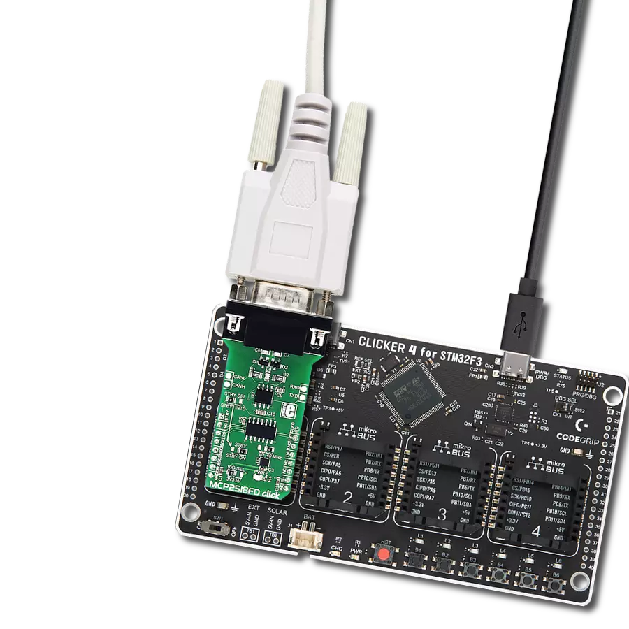
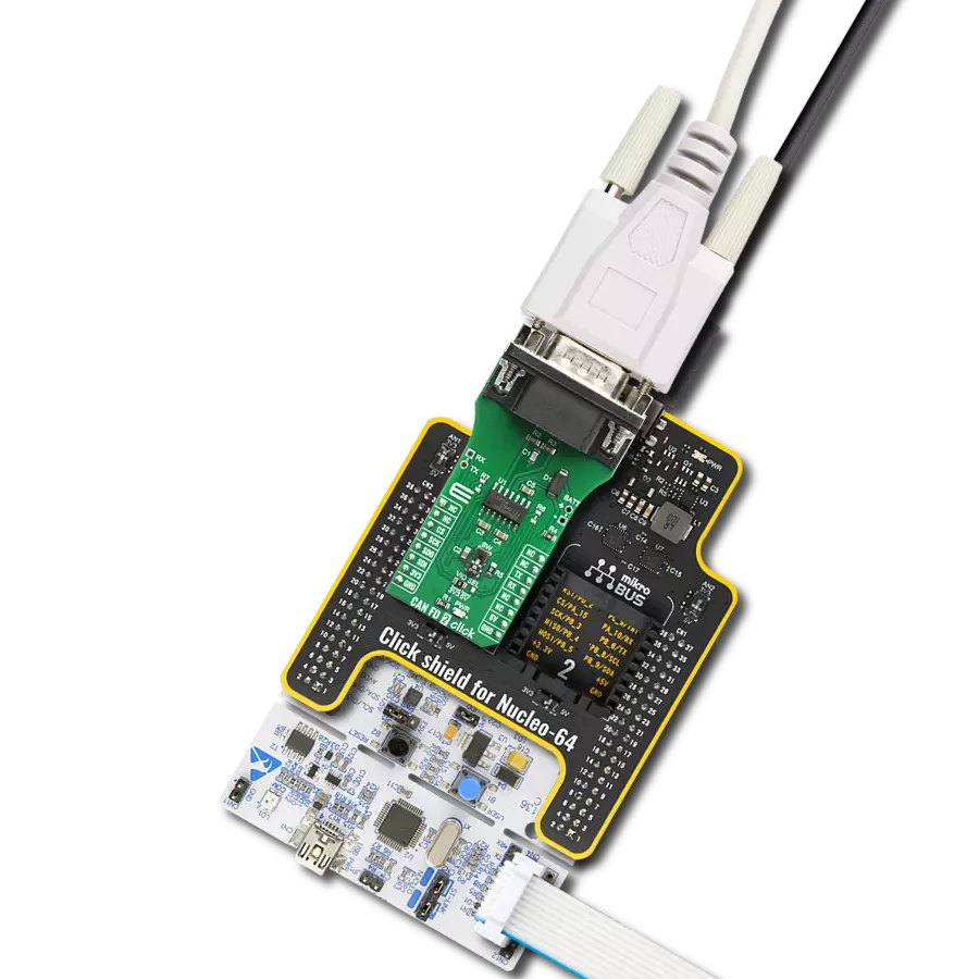
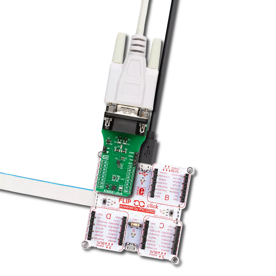
DB9 Cable Female-to-Female (2m) cable is essential for establishing dependable serial data connections between devices. With its DB9 female connectors on both ends, this cable enables a seamless link between various equipment, such as computers, routers, switches, and other serial devices. Measuring 2 meters in length, it offers flexibility in arranging your setup without compromising data transmission quality. Crafted with precision, this cable ensures consistent and reliable data exchange, making it suitable for industrial applications, office environments, and home setups. Whether configuring networking equipment, accessing console ports, or utilizing serial peripherals, this cable's durable construction and robust connectors guarantee a stable connection. Simplify your data communication needs with the 2m DB9 female-to-female cable, an efficient solution designed to meet your serial connectivity requirements easily and efficiently.

Used MCU Pins
mikroBUS™ mapper
Take a closer look
Click board™ Schematic

Step by step
Project assembly
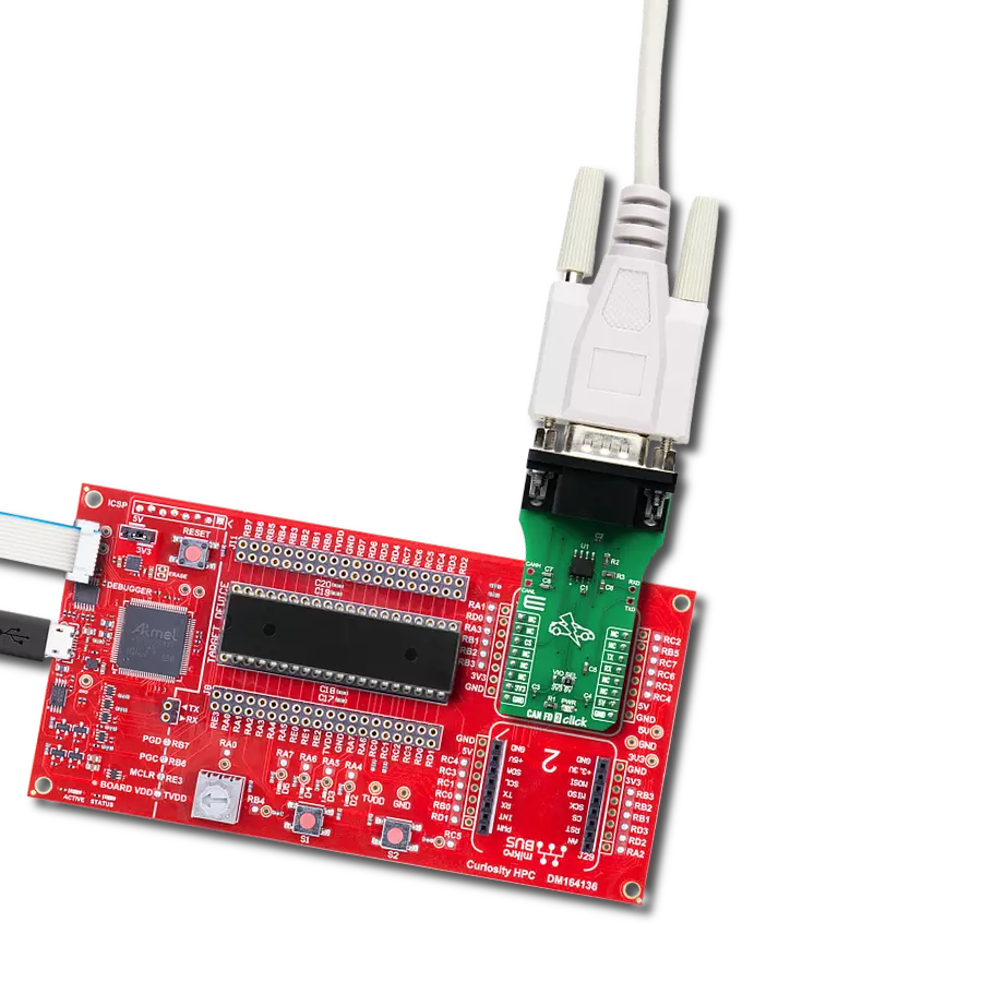
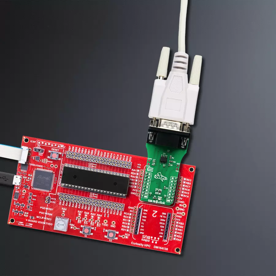
Start by selecting your development board and Click board™. Begin with the Curiosity HPC as your development board.


Software Support
Library Description
This library contains API for CAN FD 3 Click driver.
Key functions:
canfd3_generic_read- Generic read functioncanfd3_generic_write- Generic write functioncanfd3_set_cs_pin- Sets the CS pin state.
Open Source
Code example
The complete application code and a ready-to-use project are available through the NECTO Studio Package Manager for direct installation in the NECTO Studio. The application code can also be found on the MIKROE GitHub account.
/*!
 * \file
 * \brief CanFd3 Click example
 *
 * # Description
 * This example reads and processes data from CAN FD 3 Clicks.
 *
 * The demo application is composed of two sections :
 *
 * ## Application Init
 * Initializes the driver and enables the Click board.
 *
 * ## Application Task
 * Depending on the selected mode, it reads all the received data or sends the desired message
 * every 2 seconds.
 *
 * ## Additional Function
 * - canfd3_process ( ) - The general process of collecting the received data.
 *
 * \author MikroE Team
 *
 */
// ------------------------------------------------------------------- INCLUDES

#include "board.h"
#include "log.h"
#include "canfd3.h"
#include "string.h"

#define PROCESS_RX_BUFFER_SIZE 500

#define TEXT_TO_SEND "MikroE\r\n"

// ------------------------------------------------------------------ VARIABLES

// #define DEMO_APP_RECEIVER
#define DEMO_APP_TRANSMITTER

static canfd3_t canfd3;
static log_t logger;

// ------------------------------------------------------- ADDITIONAL FUNCTIONS

static void canfd3_process ( void )
{
    int32_t rsp_size;

    char uart_rx_buffer[ PROCESS_RX_BUFFER_SIZE ] = { 0 };
    uint8_t check_buf_cnt;

    rsp_size = canfd3_generic_read( &canfd3, uart_rx_buffer, PROCESS_RX_BUFFER_SIZE );

    if ( rsp_size > 0 )
    {
        for ( check_buf_cnt = 0; check_buf_cnt < rsp_size; check_buf_cnt++ )
        {
            log_printf( &logger, "%c", uart_rx_buffer[ check_buf_cnt ] );
        }
    }
    Delay_ms ( 100 );
}

// ------------------------------------------------------ APPLICATION FUNCTIONS

void application_init ( void )
{
    log_cfg_t log_cfg;
    canfd3_cfg_t cfg;

    /**
     * Logger initialization.
     * Default baud rate: 115200
     * Default log level: LOG_LEVEL_DEBUG
     * @note If USB_UART_RX and USB_UART_TX
     * are defined as HAL_PIN_NC, you will
     * need to define them manually for log to work.
     * See @b LOG_MAP_USB_UART macro definition for detailed explanation.
     */
    LOG_MAP_USB_UART( log_cfg );
    log_init( &logger, &log_cfg );
    log_info( &logger, "---- Application Init ----" );

    //  Click initialization.

    canfd3_cfg_setup( &cfg );
    CANFD3_MAP_MIKROBUS( cfg, MIKROBUS_1 );
    canfd3_init( &canfd3, &cfg );

    canfd3_set_cs_pin( &canfd3, CANFD3_MODE_NORMAL );
    Delay_ms ( 100 );
}

void application_task ( void )
{
#ifdef DEMO_APP_RECEIVER
    canfd3_process( );
#endif
#ifdef DEMO_APP_TRANSMITTER
    canfd3_generic_write( &canfd3, TEXT_TO_SEND, 8 );
    log_info( &logger, "--- The message is sent ---" );
    Delay_ms ( 1000 );
    Delay_ms ( 1000 );
#endif
}
int main ( void )
{
    /* Do not remove this line or clock might not be set correctly. */
    #ifdef PREINIT_SUPPORTED
    preinit();
    #endif

    application_init( );

    for ( ; ; )
    {
        application_task( );
    }

    return 0;
}

// ------------------------------------------------------------------------ END
Additional Support
Resources
Category:CAN