Experience voltage stability with LM317 and PIC32MZ2048EFH100
Classic voltage regulator

Published Jul 31, 2023
Click board™
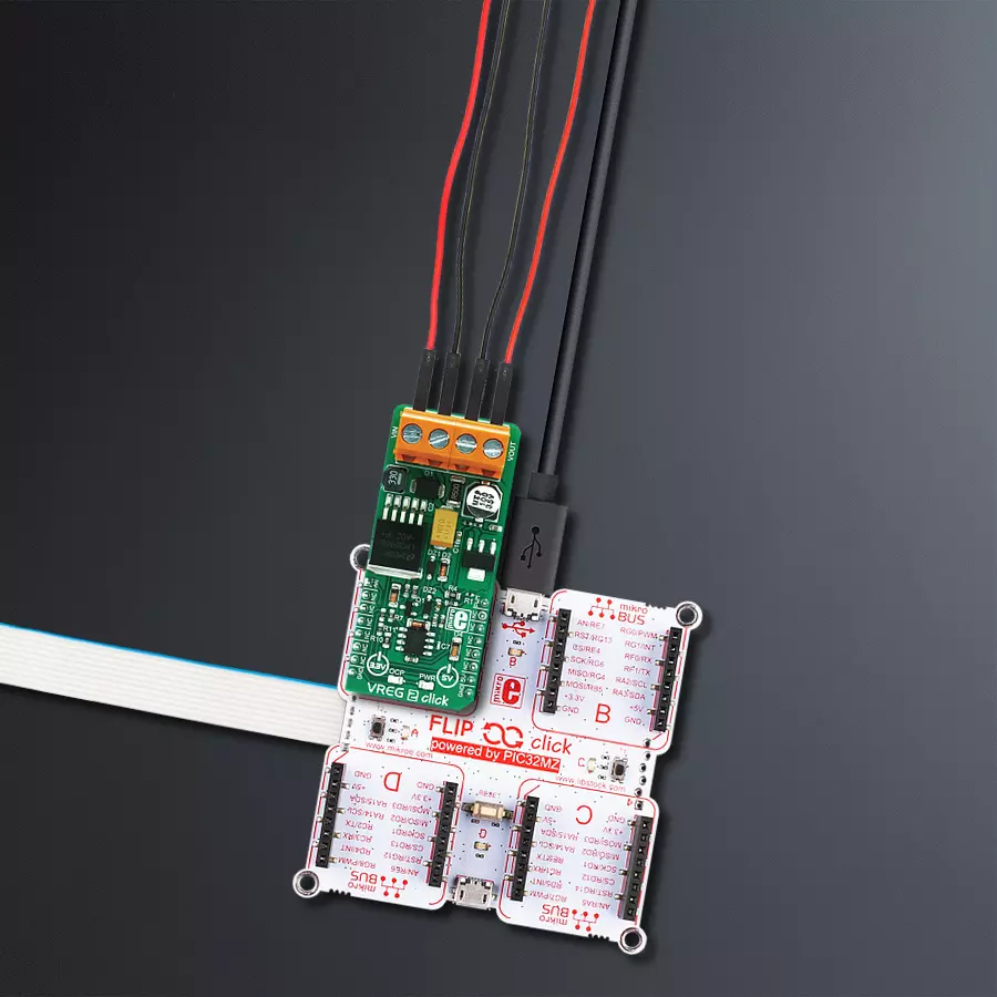
VREG 2 Click
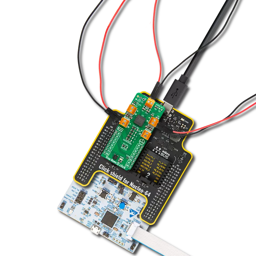
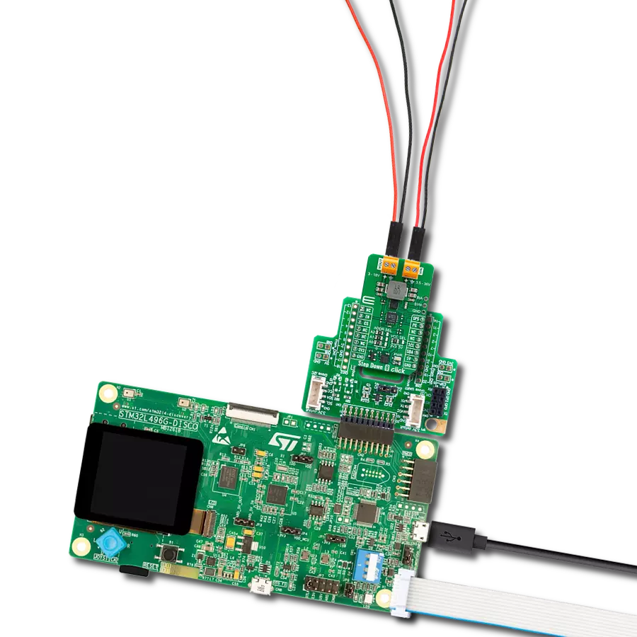
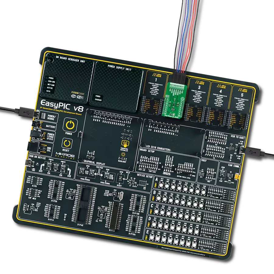
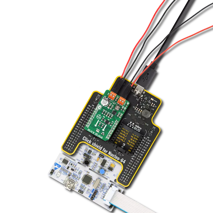
Dev. board
Flip&Click PIC32MZ
Compiler
NECTO Studio
MCU
PIC32MZ2048EFH100
Efficient, reliable, and ready to take your devices to the next level!
A
A
Hardware Overview
How does it work?
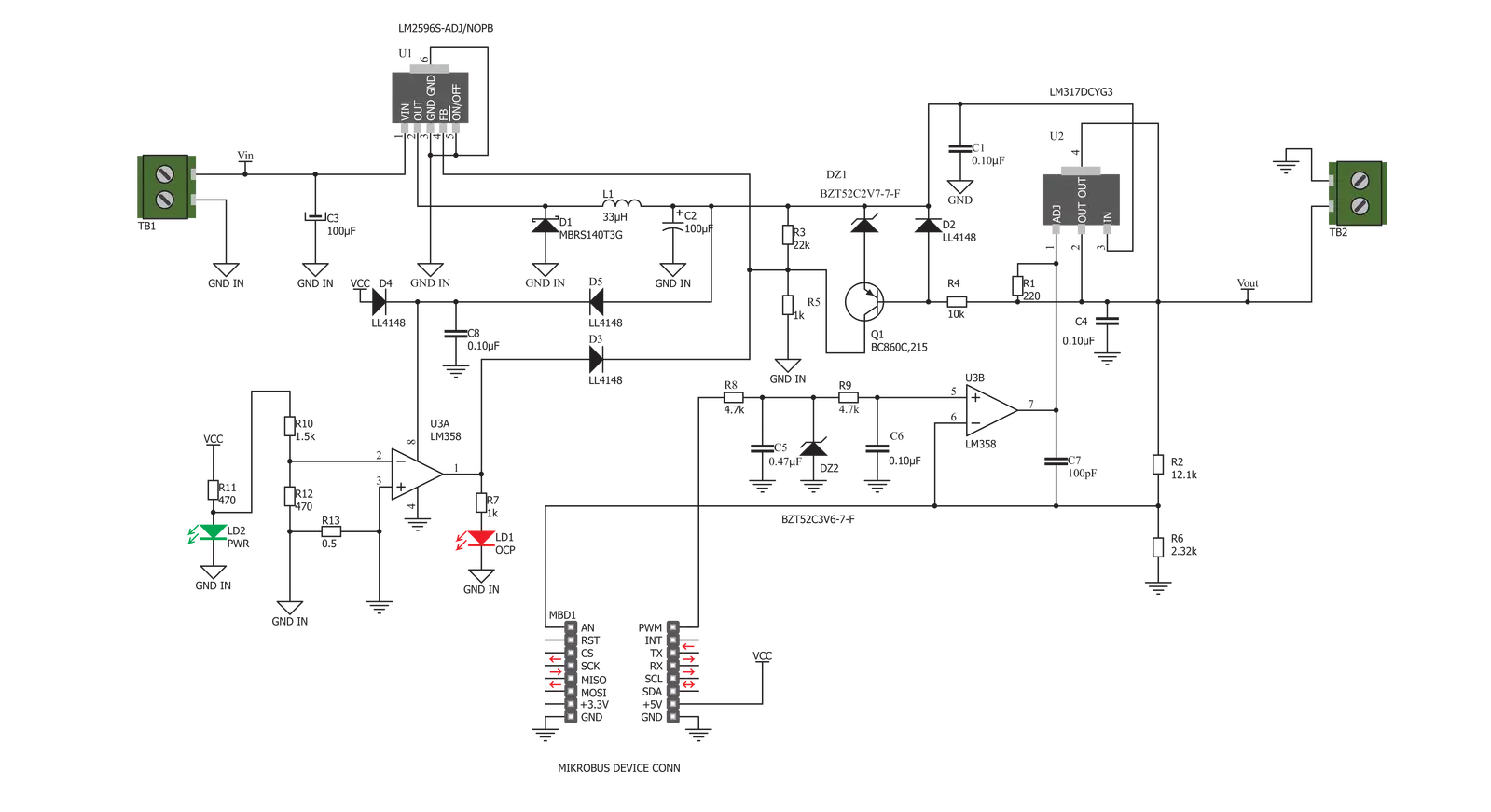
VREG 2 Click is based on the outstanding performance of the LM317, a well-established adjustable voltage regulator from Texas Instruments. The circuit on this Click board™ consists of two voltage regulators, one of which is a linear voltage regulator. At the same time the second is a switching step-down converter, also known as the buck converter. Such topology combines the benefits of both worlds: linear regulator offers low voltage ripple and noise, while the switching regulator provides optimal working conditions, avoiding large voltage differences between the input and output voltage of the linear regulator. Unlike the buck converter, a significant difference between the linear regulator's input and output voltage leads to significant dissipation losses. The Click board™ also uses the LM2596, a 3A step-down voltage regulator working at 150 kHz, from Texas Instruments. It belongs to the Simple Switcher™ line of products and supports both continuous and discontinuous modes. This buck DC-DC
converter can handle from 4.5V up to 40V, but the circuit works reliably with voltages between 9V and 35V. This IC has a reasonably simple layout with just a few external pins. The feedback loop regulates the output voltage of the DC-DC converter. Normally, there is a voltage divider with its center pin routed to the FB pin of the LM2596, but on this Click board™, there is a PNP BJT with the 2.7V Zener diode on its emitter, which is used to provide about 3V more voltage on its output, than the desired target voltage. This provides an ideal voltage headroom for the linear regulator, allowing for greater efficiency and less power dissipation. The input voltage is provided from the LM2596, and as already mentioned, this voltage is about 3V greater than the target regulation voltage, allowing optimal headroom for LM317 IC. The ADJ pin is used to set the output voltage on this IC. The output of the first op-amp of the LM358 IC, a dual operational amplifier from Texas Instruments, drives it. The PWM signal from the MCU controls this op-amp's non-inverting
input; therefore, the mikroBUS™ PWM pin is routed to this non-inverting input. By applying an additional RC filter, the PWM signal is converted to a constant linear voltage ranging up to 3.3V, as it is limited by another Zener diode on this input. The inverting pin of this op-amp is connected to an output voltage divider, with its center tap at 3.3V for the maximum output voltage of 15V. This allows the output voltage to be measured by the host MCU. Therefore, this pin is routed to the mikroBUS™ AN pin. The short circuit protection section is designed with the second op-amp of the LM358 IC, working as a comparator. When the current starts flowing through the 0.5Ω resistor, in the event of a short circuit on the output, it will cause the op-amp output voltage to rise. The red LED indicator labeled OCP will be lit, indicating the short circuit condition. This will also cause the rising of the FB voltage of the buck regulator, effectively blocking its operation and cutting the power to the output.

Features overview
Development board
Flip&Click PIC32MZ is a compact development board designed as a complete solution that brings the flexibility of add-on Click boards™ to your favorite microcontroller, making it a perfect starter kit for implementing your ideas. It comes with an onboard 32-bit PIC32MZ microcontroller, the PIC32MZ2048EFH100 from Microchip, four mikroBUS™ sockets for Click board™ connectivity, two USB connectors, LED indicators, buttons, debugger/programmer connectors, and two headers compatible with Arduino-UNO pinout. Thanks to innovative manufacturing technology,
it allows you to build gadgets with unique functionalities and features quickly. Each part of the Flip&Click PIC32MZ development kit contains the components necessary for the most efficient operation of the same board. In addition, there is the possibility of choosing the Flip&Click PIC32MZ programming method, using the chipKIT bootloader (Arduino-style development environment) or our USB HID bootloader using mikroC, mikroBasic, and mikroPascal for PIC32. This kit includes a clean and regulated power supply block through the USB Type-C (USB-C) connector. All communication
methods that mikroBUS™ itself supports are on this board, including the well-established mikroBUS™ socket, user-configurable buttons, and LED indicators. Flip&Click PIC32MZ development kit allows you to create a new application in minutes. Natively supported by Mikroe software tools, it covers many aspects of prototyping thanks to a considerable number of different Click boards™ (over a thousand boards), the number of which is growing every day.

Microcontroller Overview
MCU Card / MCU
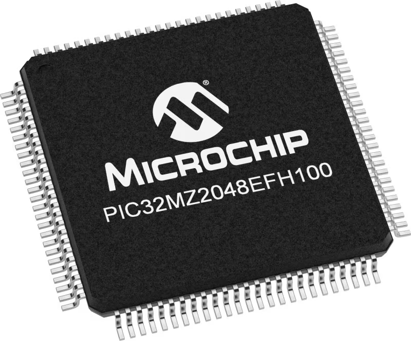
Architecture
PIC32
MCU Memory (KB)
2048
Silicon Vendor
Microchip
Pin count
100
RAM (Bytes)
524288
Used MCU Pins
mikroBUS™ mapper
Take a closer look
Click board™ Schematic
Step by step
Project assembly

Start by selecting your development board and Click board™. Begin with the Flip&Click PIC32MZ as your development board.


Track your results in real time
Application Output
1. Application Output - In Debug mode, the 'Application Output' window enables real-time data monitoring, offering direct insight into execution results. Ensure proper data display by configuring the environment correctly using the provided tutorial.

2. UART Terminal - Use the UART Terminal to monitor data transmission via a USB to UART converter, allowing direct communication between the Click board™ and your development system. Configure the baud rate and other serial settings according to your project's requirements to ensure proper functionality. For step-by-step setup instructions, refer to the provided tutorial.

3. Plot Output - The Plot feature offers a powerful way to visualize real-time sensor data, enabling trend analysis, debugging, and comparison of multiple data points. To set it up correctly, follow the provided tutorial, which includes a step-by-step example of using the Plot feature to display Click board™ readings. To use the Plot feature in your code, use the function: plot(*insert_graph_name*, variable_name);. This is a general format, and it is up to the user to replace 'insert_graph_name' with the actual graph name and 'variable_name' with the parameter to be displayed.

Software Support
Library Description
This library contains API for VREG 2 Click driver.
Key functions:
vreg2_set_duty_cycle- This function sets the PWM duty cycle in percentagesvreg2_pwm_start- This function starts the PWM module outputvreg2_pwm_stop- This function stops the PWM module output
Open Source
Code example
The complete application code and a ready-to-use project are available through the NECTO Studio Package Manager for direct installation in the NECTO Studio. The application code can also be found on the MIKROE GitHub account.
/*!
 * @file main.c
 * @brief VREG 2 Click example
 *
 * # Description
 * This example demonstrates the use of the VREG 2 Click board by changing
 * the voltage output every 5 seconds.
 *
 * The demo application is composed of two sections :
 *
 * ## Application Init
 * Initializes the driver and performs the Click default configuration.
 *
 * ## Application Task
 * Controls the voltage output by changing the PWM duty cycle every 5 seconds.
 * The duty cycle ranges from 10% to 50%. Each step will be logged on
 * the USB UART where you can track the program flow.
 *
 * @author Stefan Filipovic
 *
 */

#include "board.h"
#include "log.h"
#include "vreg2.h"

static vreg2_t vreg2;
static log_t logger;

void application_init ( void )
{
    log_cfg_t log_cfg;  /**< Logger config object. */
    vreg2_cfg_t vreg2_cfg;  /**< Click config object. */

    /**
     * Logger initialization.
     * Default baud rate: 115200
     * Default log level: LOG_LEVEL_DEBUG
     * @note If USB_UART_RX and USB_UART_TX
     * are defined as HAL_PIN_NC, you will
     * need to define them manually for log to work.
     * See @b LOG_MAP_USB_UART macro definition for detailed explanation.
     */
    LOG_MAP_USB_UART( log_cfg );
    log_init( &logger, &log_cfg );
    log_info( &logger, " Application Init " );

    // Click initialization.
    vreg2_cfg_setup( &vreg2_cfg );
    VREG2_MAP_MIKROBUS( vreg2_cfg, MIKROBUS_1 );
    if ( PWM_ERROR == vreg2_init( &vreg2, &vreg2_cfg ) )
    {
        log_error( &logger, " Communication init." );
        for ( ; ; );
    }

    if ( VREG2_ERROR == vreg2_default_cfg ( &vreg2 ) )
    {
        log_error( &logger, " Default configuration." );
        for ( ; ; );
    }

    log_info( &logger, " Application Task " );
}

void application_task ( void )
{
    static int8_t duty_pct = 10;
    static int8_t duty_step = 10;
    if ( VREG2_OK == vreg2_set_duty_cycle ( &vreg2, ( float ) duty_pct / 100 ) )
    {
        log_printf( &logger, "\r\n Duty: %u%%\r\n", ( uint16_t ) duty_pct );
    }
    duty_pct += duty_step;
    if ( ( duty_pct > 50 ) || ( duty_pct < 10 ) )
    {
        duty_step = -duty_step;
        duty_pct += ( duty_step * 2 );
    }
    Delay_ms ( 1000 );
    Delay_ms ( 1000 );
    Delay_ms ( 1000 );
    Delay_ms ( 1000 );
    Delay_ms ( 1000 );
}

int main ( void )
{
    /* Do not remove this line or clock might not be set correctly. */
    #ifdef PREINIT_SUPPORTED
    preinit();
    #endif

    application_init( );

    for ( ; ; )
    {
        application_task( );
    }

    return 0;
}

// ------------------------------------------------------------------------ END