Experience the power of efficient signal conversion with ADS8665 and PIC32MZ2048EFM100
From analog to awesome

Published Nov 13, 2023
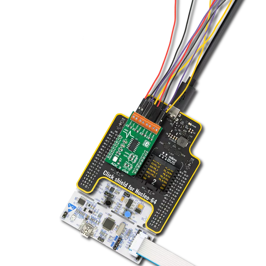
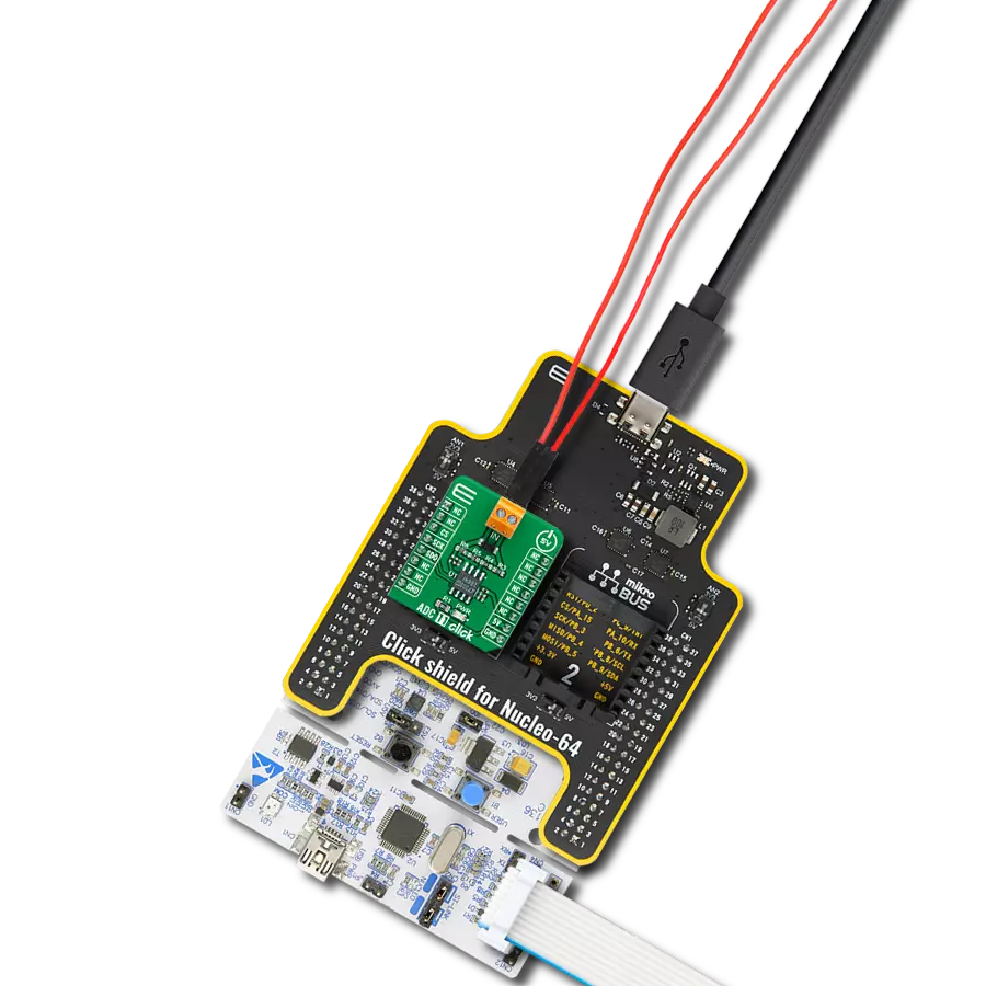
Click board™
ADC 22 Click
Dev. board
Curiosity PIC32 MZ EF
Compiler
NECTO Studio
MCU
PIC32MZ2048EFM100
Our analog-to-digital converter seamlessly transforms complex analog signals into precise digital data, ensuring unparalleled accuracy in every conversion.
A
A
Hardware Overview
How does it work?
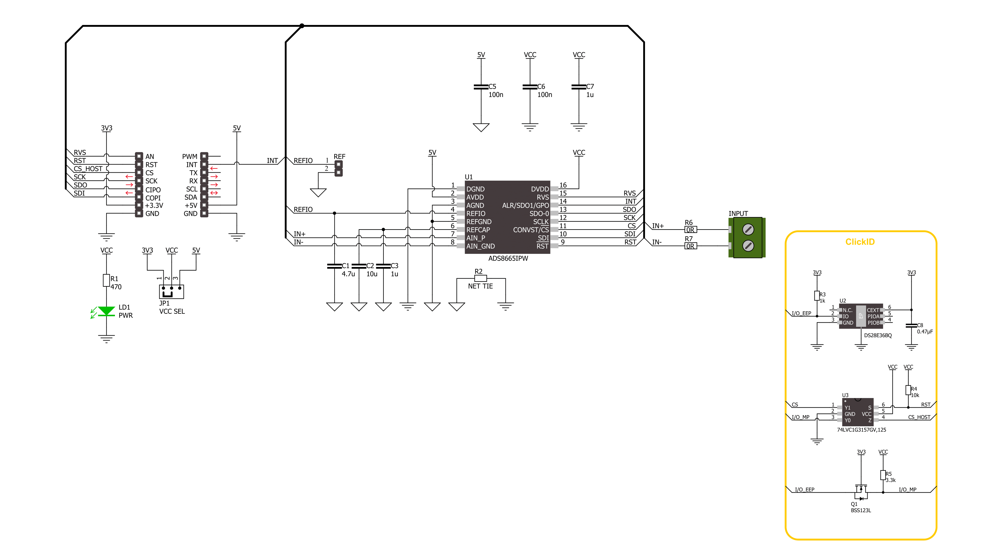
ADC 22 Click is based on the ADS8665, a 12-bit high-speed single-supply SAR ADC data acquisition system with programmable bipolar input ranges from Texas Instruments. This ADC operates on a single 5V supply used from the mikroBUS™ power rail and supports true bipolar input ranges of ±12.288V, ±6.144V, ±10.24V, ±5.12V, and ±2.56V, as well as unipolar input ranges of 0 to 12.288V, or 10.24V, 6.144V, and 5.12V. The gain and offset errors are accurately trimmed within specified values to ensure a high DC precision for each input range. The input range selection is made by software. The ADC features an overvoltage protection circuit of up to ±20V and an on-chip 4.096V reference with extremely low-temperature drift. In addition, ADC 22 Click is equipped with an external voltage reference REF header, which allows you to apply voltages to
ADS8665 ADC from 4.046 up to 4.146V. You can separate the grounds for external voltage reference usage by desoldering the NET TIE R2 resistor. The ADC 22 Click features alarm functions that consist of an input alarm and an AVDD supply alarm. The alarm function should be enabled over the software, thus enabling both alarm functions by default. You can later separately disable one of them. Another neat feature of this Click board™ is the RVS multi-function output pin, which, regarding the CS pin status, can reflect the status of the internal ADCST signal or the status of the RVS depending on the output protocol selection. The device allows the output clock on the RVS pin to be synchronous to either the external clock provided on the SCLK pin or to the device's internal clock. In all SRC modes of operation, the RVS pin provides the output clock, synchronous to
the device data output. The RVS pin can be monitored for timing benefits. ADC 22 Click uses a standard 4-Wire SPI serial interface to communicate with the host MCU supporting high serial clock frequency. It also supports an enhanced SPI interface (multiSPI) that maximizes the sampling rate even with lower-speed host controllers. The alarm interrupt is available on the INT pin, and you can reset the device over the RST pin. The RVS pin is a multi-function pin for the serial interface. This Click board™ can operate with either 3.3V or 5V logic voltage levels selected via the VCC SEL jumper. This way, both 3.3V and 5V capable MCUs can use the communication lines properly. Also, this Click board™ comes equipped with a library containing easy-to-use functions and an example code that can be used as a reference for further development.

Features overview
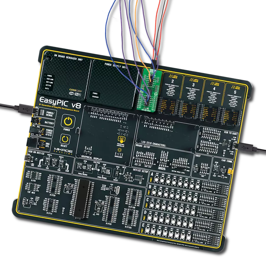
Development board
Curiosity PIC32 MZ EF development board is a fully integrated 32-bit development platform featuring the high-performance PIC32MZ EF Series (PIC32MZ2048EFM) that has a 2MB Flash, 512KB RAM, integrated FPU, Crypto accelerator, and excellent connectivity options. It includes an integrated programmer and debugger, requiring no additional hardware. Users can expand
functionality through MIKROE mikroBUS™ Click™ adapter boards, add Ethernet connectivity with the Microchip PHY daughter board, add WiFi connectivity capability using the Microchip expansions boards, and add audio input and output capability with Microchip audio daughter boards. These boards are fully integrated into PIC32’s powerful software framework, MPLAB Harmony,
which provides a flexible and modular interface to application development a rich set of inter-operable software stacks (TCP-IP, USB), and easy-to-use features. The Curiosity PIC32 MZ EF development board offers expansion capabilities making it an excellent choice for a rapid prototyping board in Connectivity, IOT, and general-purpose applications.

Microcontroller Overview
MCU Card / MCU
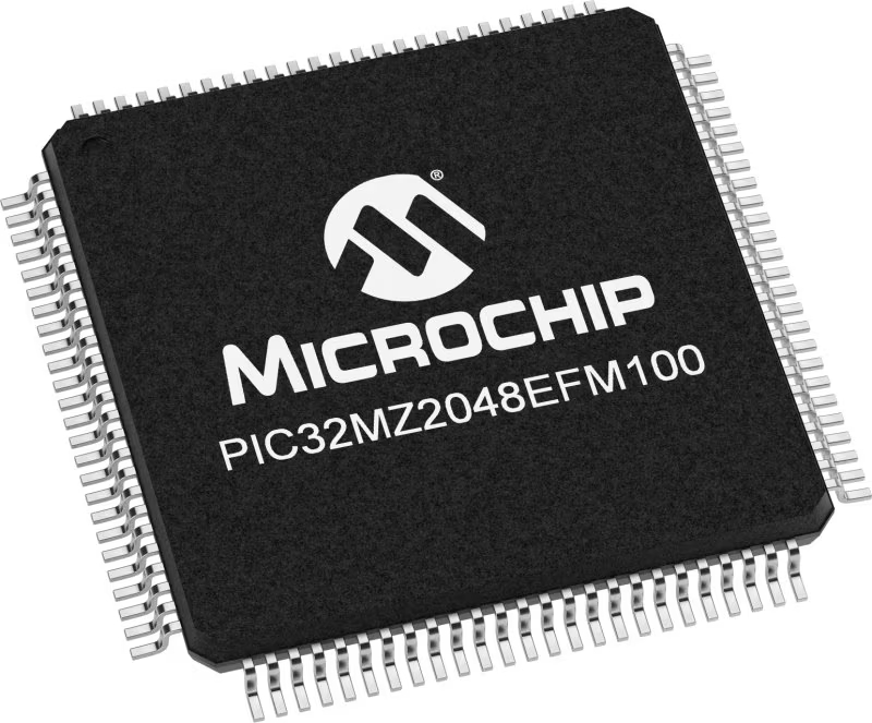
Architecture
PIC32
MCU Memory (KB)
2048
Silicon Vendor
Microchip
Pin count
100
RAM (Bytes)
524288
Used MCU Pins
mikroBUS™ mapper
Take a closer look
Click board™ Schematic
Step by step
Project assembly

Start by selecting your development board and Click board™. Begin with the Curiosity PIC32 MZ EF as your development board.


Track your results in real time
Application Output
1. Application Output - In Debug mode, the 'Application Output' window enables real-time data monitoring, offering direct insight into execution results. Ensure proper data display by configuring the environment correctly using the provided tutorial.

2. UART Terminal - Use the UART Terminal to monitor data transmission via a USB to UART converter, allowing direct communication between the Click board™ and your development system. Configure the baud rate and other serial settings according to your project's requirements to ensure proper functionality. For step-by-step setup instructions, refer to the provided tutorial.

3. Plot Output - The Plot feature offers a powerful way to visualize real-time sensor data, enabling trend analysis, debugging, and comparison of multiple data points. To set it up correctly, follow the provided tutorial, which includes a step-by-step example of using the Plot feature to display Click board™ readings. To use the Plot feature in your code, use the function: plot(*insert_graph_name*, variable_name);. This is a general format, and it is up to the user to replace 'insert_graph_name' with the actual graph name and 'variable_name' with the parameter to be displayed.

Software Support
Library Description
This library contains API for ADC 22 Click driver.
Key functions:
adc22_get_voltage- ADC 22 get voltage level function.adc22_get_adc_raw_data- ADC 22 get ADC raw data function.adc22_set_range- ADC 22 set range function.
Open Source
Code example
The complete application code and a ready-to-use project are available through the NECTO Studio Package Manager for direct installation in the NECTO Studio. The application code can also be found on the MIKROE GitHub account.
/*!
 * @file main.c
 * @brief ADC 22 Click example
 *
 * # Description
 * This example demonstrates the use of the ADC 22 Click board™
 * by reading and writing data by using SPI serial interface and reading results of AD conversion.
 *
 * The demo application is composed of two sections :
 *
 * ## Application Init
 * Initialization of SPI module and log UART.
 * After driver initialization, the app executes a default configuration.
 *
 * ## Application Task
 * The demo application reads the voltage levels from analog input and displays the results.
 * By default, the operating input range sets from 0V to 12.288V [3×Vref;Vref=4.096V].
 * Results are being sent to the UART Terminal, where you can track their changes.
 *
 * @author Nenad Filipovic
 *
 */

#include "board.h"
#include "log.h"
#include "adc22.h"

static adc22_t adc22;
static log_t logger;

void application_init ( void )
{
    log_cfg_t log_cfg;  /**< Logger config object. */
    adc22_cfg_t adc22_cfg;  /**< Click config object. */

    /**
     * Logger initialization.
     * Default baud rate: 115200
     * Default log level: LOG_LEVEL_DEBUG
     * @note If USB_UART_RX and USB_UART_TX
     * are defined as HAL_PIN_NC, you will
     * need to define them manually for log to work.
     * See @b LOG_MAP_USB_UART macro definition for detailed explanation.
     */
    LOG_MAP_USB_UART( log_cfg );
    log_init( &logger, &log_cfg );
    log_info( &logger, " Application Init " );

    // Click initialization.
    adc22_cfg_setup( &adc22_cfg );
    ADC22_MAP_MIKROBUS( adc22_cfg, MIKROBUS_1 );
    if ( SPI_MASTER_ERROR == adc22_init( &adc22, &adc22_cfg ) )
    {
        log_error( &logger, " Communication init." );
        for ( ; ; );
    }
    Delay_ms ( 100 );

    if ( ADC22_ERROR == adc22_default_cfg ( &adc22 ) )
    {
        log_error( &logger, " Default configuration." );
        for ( ; ; );
    }
    Delay_ms ( 100 );

    log_info( &logger, " Application Task " );
    log_printf( &logger, " ----------------\r\n" );
    Delay_ms ( 100 );
}

void application_task ( void )
{
    static float voltage = 0.0;
    if ( ADC22_OK == adc22_get_voltage ( &adc22, &voltage ) )
    {
        log_printf( &logger, " Voltage : %.2f V\r\n", voltage );
        log_printf( &logger, " ----------------\r\n" );
        Delay_ms ( 1000 );
    }
}

int main ( void )
{
    /* Do not remove this line or clock might not be set correctly. */
    #ifdef PREINIT_SUPPORTED
    preinit();
    #endif

    application_init( );

    for ( ; ; )
    {
        application_task( );
    }

    return 0;
}

// ------------------------------------------------------------------------ END