Improve your power management with LTC3129-1 and PIC18LF27K42
Revolutionary voltage control
Published Nov 01, 2023
Click board™
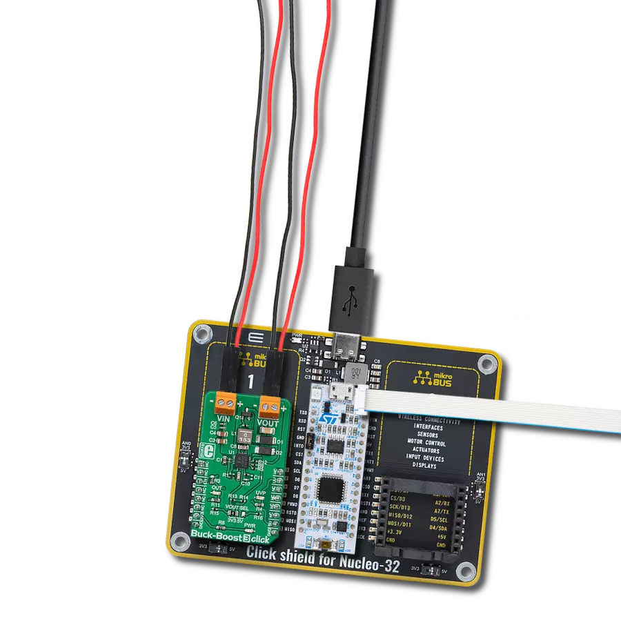
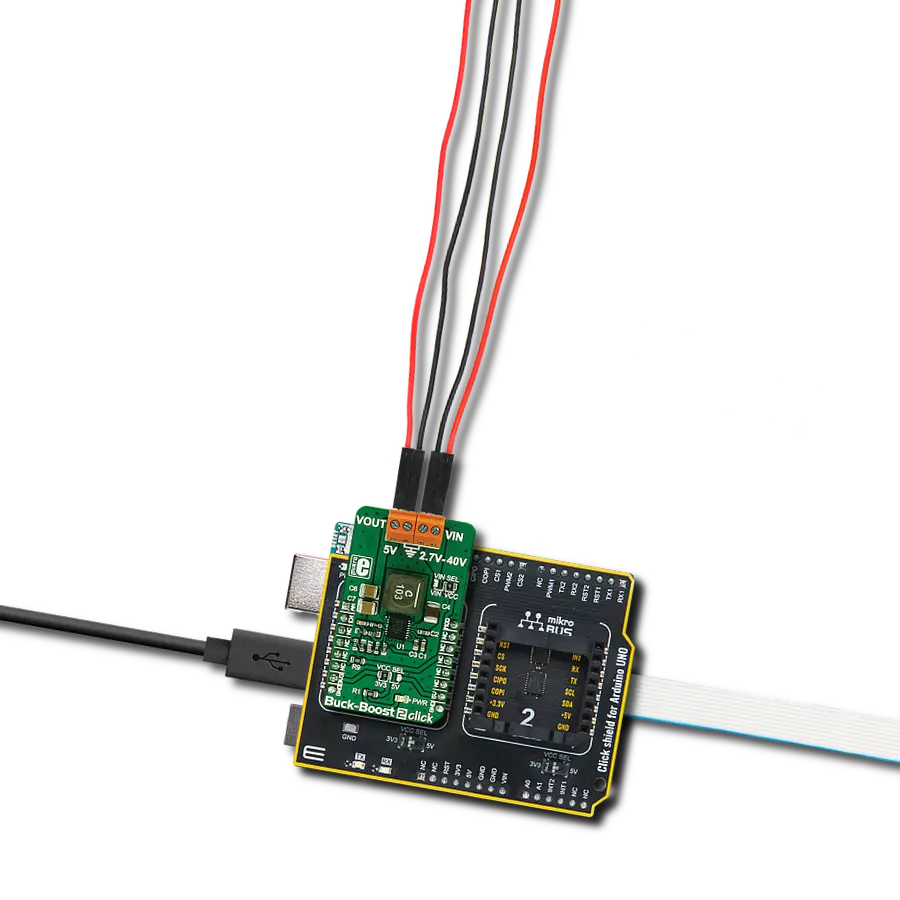
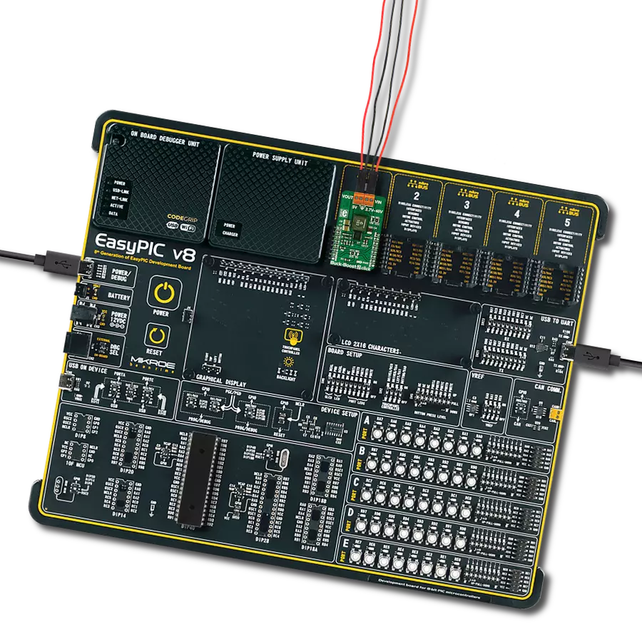
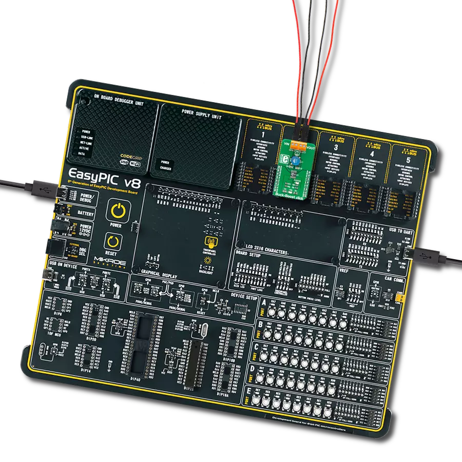
Buck-Boost Click
Dev. board
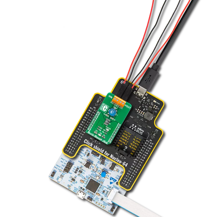
EasyPIC v8
Compiler
NECTO Studio
MCU
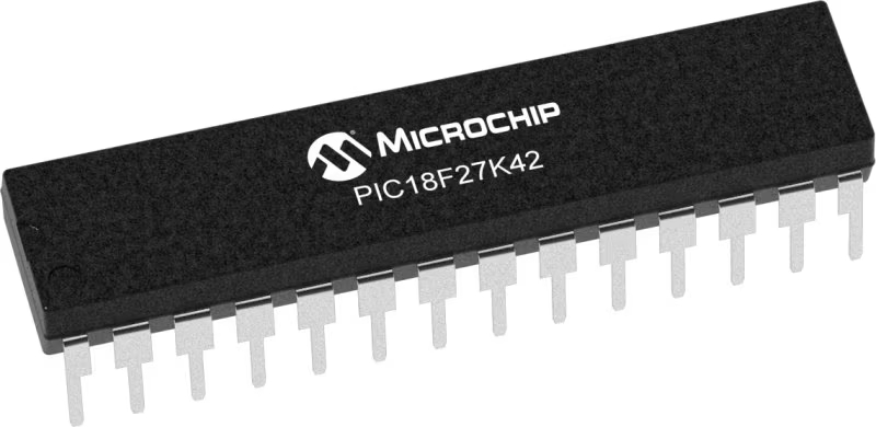
PIC18LF27K42
Your power, your rules - our Buck-Boost combo empowers you to take charge like never before.
A
A
Hardware Overview
How does it work?
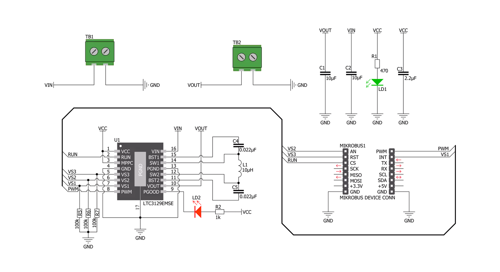
Buck-Boost Click is based on the LTC3129-1, a 1.3μA quiescent current, monolithic, current mode, buck-boost DC/DC converter that can operate over a wide input voltage range of 1.92V to 15V and provide up to 200mA to the load from Analog Devices. The LTC3129-1 is characterized by its low noise and ripple level at the output, high regulating efficiency, and low quiescent current. Eight fixed, user-programmable output voltages can be selected using the three digital programming pins routed to the INT, AN, and CS pins of the mikroBUS™ socket. A proprietary switch control algorithm allows the Buck-Boost converter to regulate output voltage with input voltages above, below, or equal to the output voltage. Transitions between the step-up or step-down operating modes are seamless and free of transients and sub-harmonic switching, making
this product ideal for noise-sensitive applications. Buck-Boost Click possesses two different modes of operation - PWM and Burst Mode, depending on the nature of the application. The PWM mode can be selected by setting the PWM pin of the mikroBUS™ socket to a logic high level and is suitable for working with higher loads connected to the converter output and when extremely low output noise is required. When selecting the PWM mode, LTC3129-1 has a fixed nominal switching frequency of 1.2MHz using an internally compensated average current mode control loop. In this mode, the output voltage's ripple and noise level are minimal. For high-efficiency operation at light loads, automatic Burst Mode operation can be selected, reducing the quiescent current to 1.3µA. Burst mode can be chosen if the PWM pin is set to a logic low level. If the connected load is
light enough, the converter will remain working in Burst mode, running only when necessary to maintain voltage regulation. Otherwise, the PWM mode will automatically engage, providing enough current for the connected load. This Click board™ completely powers itself from the VIN external power supply terminal. Once the power is applied to the VIN terminal, the circuit must also be enabled by setting the RUN pin routed to the RST pin of the mikroBUS™ socket to a high logic level. This will power up the converter, which the PWR LED indicator will indicate. It also includes additional features such as a power-good output with a Power Good LED indicator labeled PGOOD that pulls to the ground when FB drops too far below its regulated voltage. This pin also can sink up to the absolute maximum rating of 15mA when set low.

Features overview
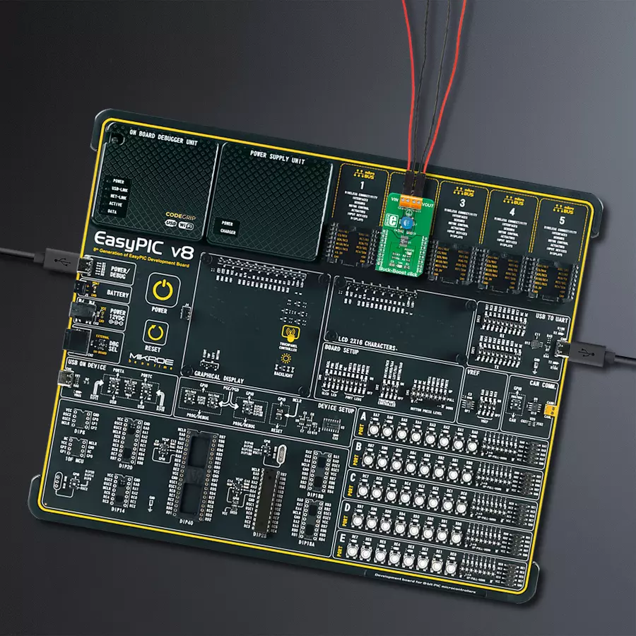
Development board
EasyPIC v8 is a development board specially designed for the needs of rapid development of embedded applications. It supports many high pin count 8-bit PIC microcontrollers from Microchip, regardless of their number of pins, and a broad set of unique functions, such as the first-ever embedded debugger/programmer. The development board is well organized and designed so that the end-user has all the necessary elements, such as switches, buttons, indicators, connectors, and others, in one place. Thanks to innovative manufacturing technology, EasyPIC v8 provides a fluid and immersive working experience, allowing access anywhere and under any
circumstances at any time. Each part of the EasyPIC v8 development board contains the components necessary for the most efficient operation of the same board. In addition to the advanced integrated CODEGRIP programmer/debugger module, which offers many valuable programming/debugging options and seamless integration with the Mikroe software environment, the board also includes a clean and regulated power supply module for the development board. It can use a wide range of external power sources, including a battery, an external 12V power supply, and a power source via the USB Type-C (USB-C) connector.
Communication options such as USB-UART, USB DEVICE, and CAN are also included, including the well-established mikroBUS™ standard, two display options (graphical and character-based LCD), and several different DIP sockets. These sockets cover a wide range of 8-bit PIC MCUs, from the smallest PIC MCU devices with only eight up to forty pins. EasyPIC v8 is an integral part of the Mikroe ecosystem for rapid development. Natively supported by Mikroe software tools, it covers many aspects of prototyping and development thanks to a considerable number of different Click boards™ (over a thousand boards), the number of which is growing every day.

Microcontroller Overview
MCU Card / MCU
Architecture
PIC
MCU Memory (KB)
128
Silicon Vendor
Microchip
Pin count
28
RAM (Bytes)
8192
Used MCU Pins
mikroBUS™ mapper
Take a closer look
Click board™ Schematic
Step by step
Project assembly

Start by selecting your development board and Click board™. Begin with the EasyPIC v8 as your development board.


Track your results in real time
Application Output
1. Application Output - In Debug mode, the 'Application Output' window enables real-time data monitoring, offering direct insight into execution results. Ensure proper data display by configuring the environment correctly using the provided tutorial.

2. UART Terminal - Use the UART Terminal to monitor data transmission via a USB to UART converter, allowing direct communication between the Click board™ and your development system. Configure the baud rate and other serial settings according to your project's requirements to ensure proper functionality. For step-by-step setup instructions, refer to the provided tutorial.

3. Plot Output - The Plot feature offers a powerful way to visualize real-time sensor data, enabling trend analysis, debugging, and comparison of multiple data points. To set it up correctly, follow the provided tutorial, which includes a step-by-step example of using the Plot feature to display Click board™ readings. To use the Plot feature in your code, use the function: plot(*insert_graph_name*, variable_name);. This is a general format, and it is up to the user to replace 'insert_graph_name' with the actual graph name and 'variable_name' with the parameter to be displayed.

Software Support
Library Description
This library contains API for Buck-Boost Click driver.
Key functions:
buckboost_set_mode_fixed_freq- This function set fixed frequency PWM operation mode of LTC3129-1buckboost_enables_auto_burst_mode- This function enables automatic burst mode operation of LTC3129-1buckboost_set_2500mv- This function set the output voltage of 2500mV
Open Source
Code example
The complete application code and a ready-to-use project are available through the NECTO Studio Package Manager for direct installation in the NECTO Studio. The application code can also be found on the MIKROE GitHub account.
/*!
 * \file
 * \brief Buck-Boost  Click example
 *
 * # Description
 * The demo application change output voltage from 2500 mV to 15000 mV every 5 seconds.
 *
 * The demo application is composed of two sections :
 *
 * ## Application Init
 * Initialization device and set default configuration.
 *
 * ## Application Task
 *  This is a example which demonstrates the use of Buck Boost Click board.
 *  Change output voltage from 2500 mV to 15000 mV every 5 seconds.
 *  All data logs write on usb uart for aproximetly every 5 sec.
 *
 * \author MikroE Team
 *
 */
// ------------------------------------------------------------------- INCLUDES

#include "board.h"
#include "log.h"
#include "buckboost.h"

// ------------------------------------------------------------------ VARIABLES

static buckboost_t buckboost;
static log_t logger;

// ------------------------------------------------------ APPLICATION FUNCTIONS

void application_init ( void )
{
    log_cfg_t log_cfg;
    buckboost_cfg_t cfg;

    /**
     * Logger initialization.
     * Default baud rate: 115200
     * Default log level: LOG_LEVEL_DEBUG
     * @note If USB_UART_RX and USB_UART_TX
     * are defined as HAL_PIN_NC, you will
     * need to define them manually for log to work.
     * See @b LOG_MAP_USB_UART macro definition for detailed explanation.
     */
    LOG_MAP_USB_UART( log_cfg );
    log_init( &logger, &log_cfg );
    log_info(&logger, "---- Application Init ----\r\n");

    //  Click initialization.

    buckboost_cfg_setup( &cfg );
    BUCKBOOST_MAP_MIKROBUS( cfg, MIKROBUS_1 );
    buckboost_init( &buckboost, &cfg );

    buckboost_default_cfg( &buckboost );
    log_printf( &logger, "--------------------------------\r\n" );
    log_printf( &logger, "        Buck Boost Click        \r\n" );
    log_printf( &logger, "--------------------------------\r\n" );
    Delay_ms ( 100 );
}

void application_task ( void )
{
    log_printf( &logger, " Set Output Voltage of  2500 mV \r\n" );
    log_printf( &logger, "--------------------------------\r\n" );
    buckboost_set_2500mv( &buckboost );
    Delay_ms ( 1000 );
    Delay_ms ( 1000 );
    Delay_ms ( 1000 );
    Delay_ms ( 1000 );
    Delay_ms ( 1000 );

    log_printf( &logger, " Set Output Voltage of  3300 mV \r\n" );
    log_printf( &logger, "--------------------------------\r\n" );
    buckboost_set_3300mv( &buckboost );
    Delay_ms ( 1000 );
    Delay_ms ( 1000 );
    Delay_ms ( 1000 );
    Delay_ms ( 1000 );
    Delay_ms ( 1000 );

    log_printf( &logger, " Set Output Voltage of  4100 mV \r\n" );
    log_printf( &logger, "--------------------------------\r\n" );
    buckboost_set_4100mv( &buckboost );
    Delay_ms ( 1000 );
    Delay_ms ( 1000 );
    Delay_ms ( 1000 );
    Delay_ms ( 1000 );
    Delay_ms ( 1000 );

    log_printf( &logger, " Set Output Voltage of  5000 mV \r\n" );
    log_printf( &logger, "--------------------------------\r\n" );
    buckboost_set_5000mv( &buckboost );
    Delay_ms ( 1000 );
    Delay_ms ( 1000 );
    Delay_ms ( 1000 );
    Delay_ms ( 1000 );
    Delay_ms ( 1000 );

    log_printf( &logger, " Set Output Voltage of  6900 mV \r\n" );
    log_printf( &logger, "--------------------------------\r\n" );
    buckboost_set_6900mv( &buckboost );
    Delay_ms ( 1000 );
    Delay_ms ( 1000 );
    Delay_ms ( 1000 );
    Delay_ms ( 1000 );
    Delay_ms ( 1000 );

    log_printf( &logger, " Set Output Voltage of  8200 mV \r\n" );
    log_printf( &logger, "--------------------------------\r\n" );
    buckboost_set_8200mv( &buckboost );
    Delay_ms ( 1000 );
    Delay_ms ( 1000 );
    Delay_ms ( 1000 );
    Delay_ms ( 1000 );
    Delay_ms ( 1000 );

    log_printf( &logger, " Set Output Voltage of  12000 mV \r\n" );
    log_printf( &logger, "--------------------------------\r\n" );
    buckboost_set_12000mv( &buckboost );
    Delay_ms ( 1000 );
    Delay_ms ( 1000 );
    Delay_ms ( 1000 );
    Delay_ms ( 1000 );
    Delay_ms ( 1000 );

    log_printf( &logger, " Set Output Voltage of  15000 mV \r\n" );
    log_printf( &logger, "--------------------------------\r\n" );
    buckboost_set_15000mv( &buckboost );
    Delay_ms ( 1000 );
    Delay_ms ( 1000 );
    Delay_ms ( 1000 );
    Delay_ms ( 1000 );
    Delay_ms ( 1000 );
}

int main ( void )
{
    /* Do not remove this line or clock might not be set correctly. */
    #ifdef PREINIT_SUPPORTED
    preinit();
    #endif

    application_init( );

    for ( ; ; )
    {
        application_task( );
    }

    return 0;
}

// ------------------------------------------------------------------------ END