Experience cutting-edge mixed-signal conversions with MAX11300 and PIC18F26K22
PIXI - Programmable mIXed signal In/out
Published Jun 08, 2023
Click board™
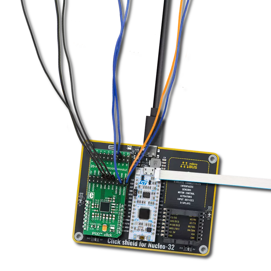
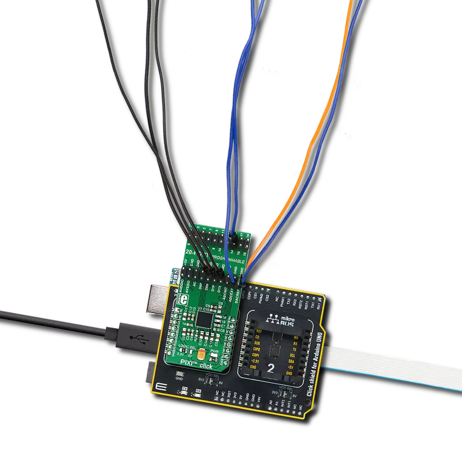
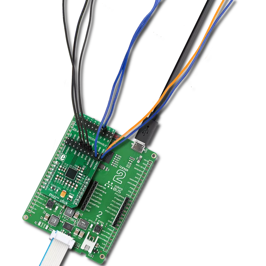
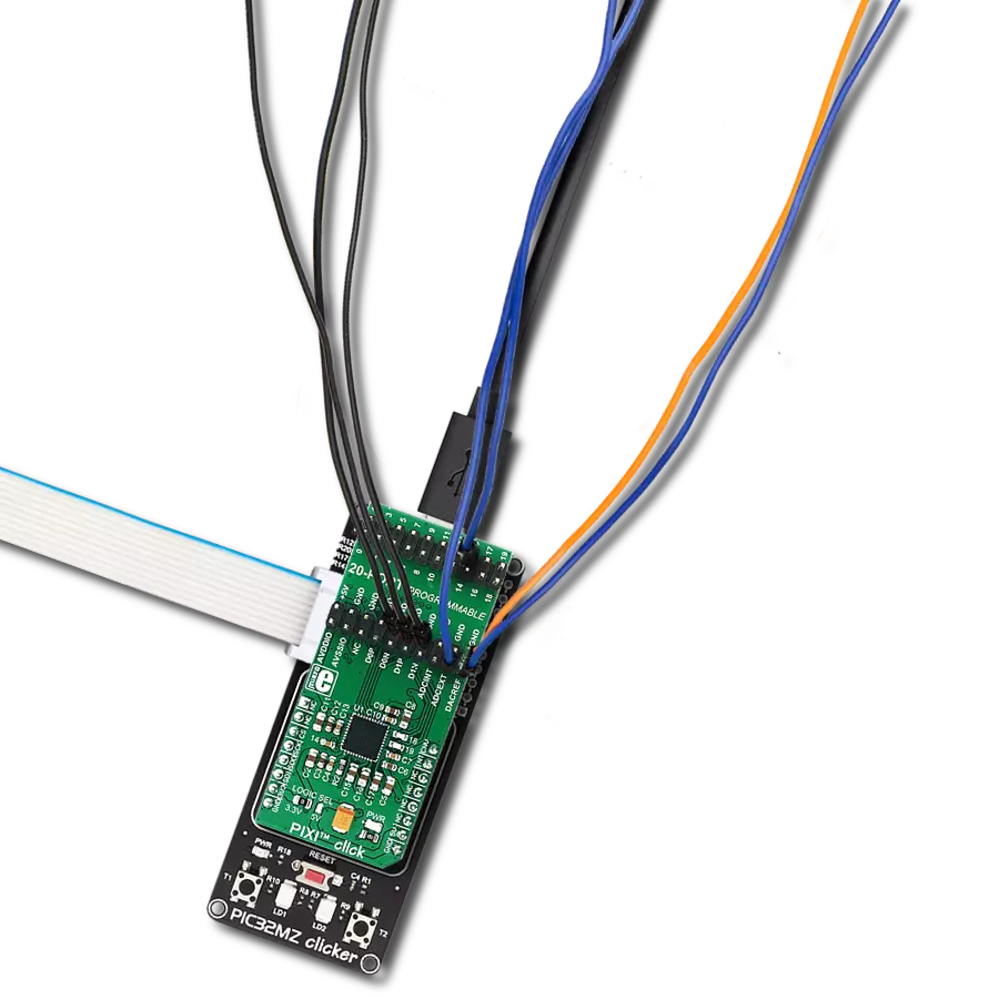
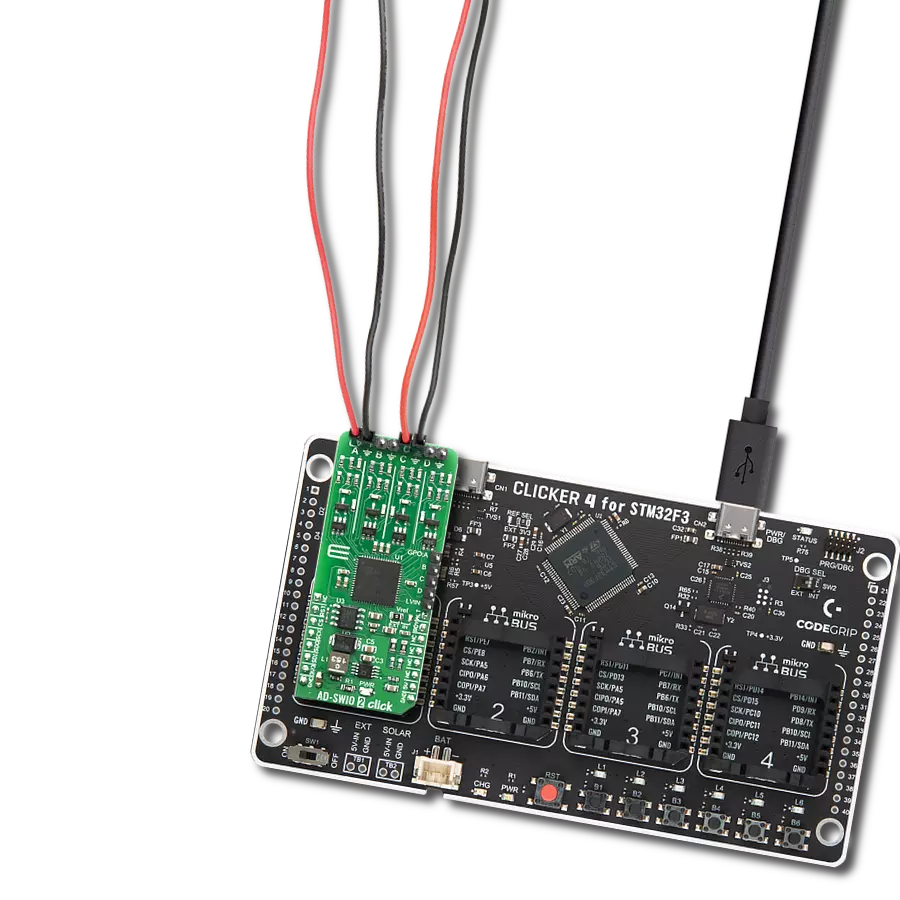
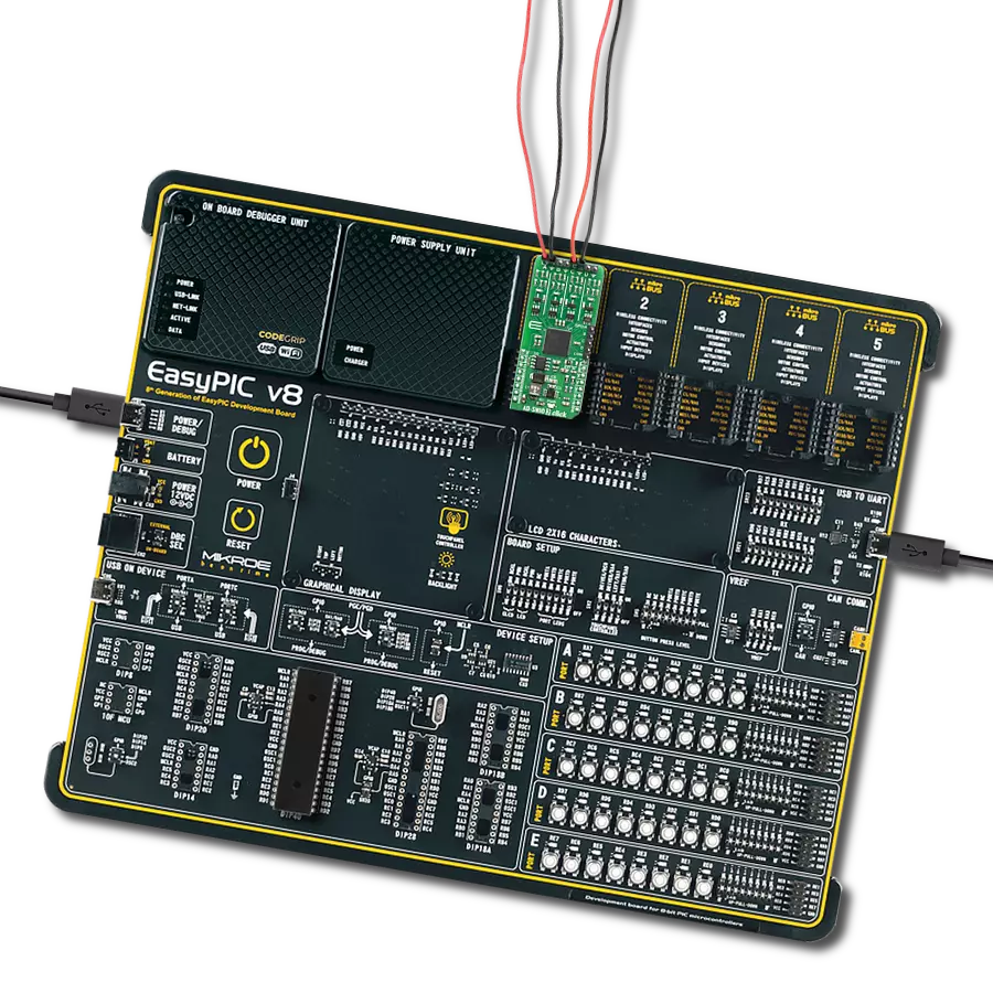
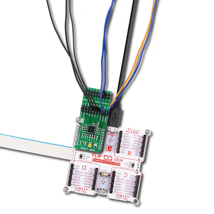
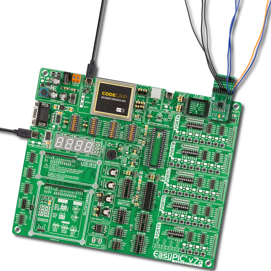
PIXI Click
Dev. board
EasyPIC v7a
Compiler
NECTO Studio
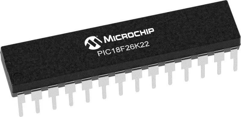
MCU
PIC18F26K22
With its 20-channel capability and versatile PIXI™ technology, our solution empowers engineers to create complex systems that demand high-performance mixed-signal data conversion
A
A
Hardware Overview
How does it work?
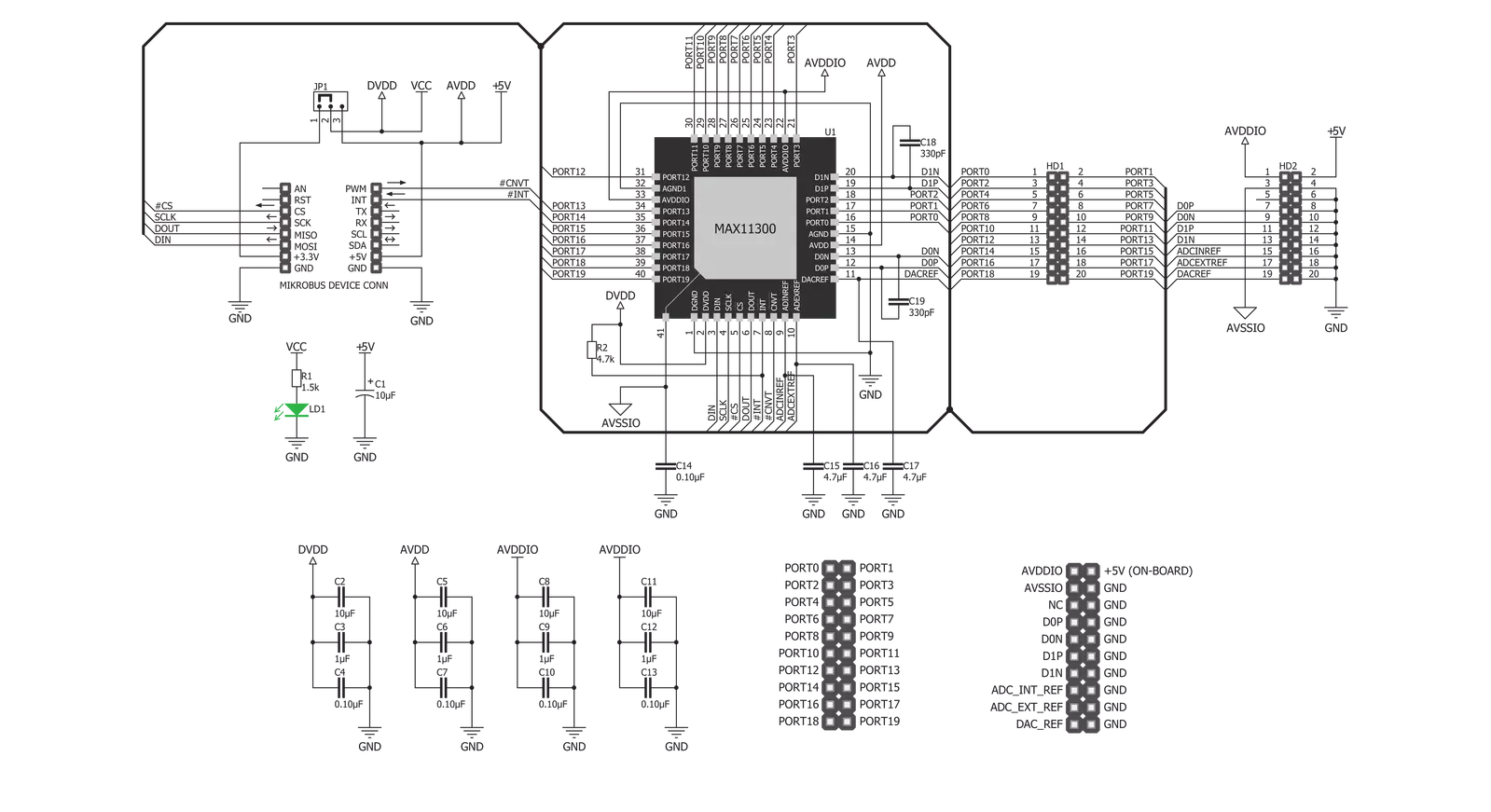
PIXI Click is based on the MAX11300 from Analog Devices. The main feature of this IC is the proprietary PIXI™ technology. PIXI™ is an abbreviation for the Programmable mIXed signal In/Out, a technology that allows very flexible routing of both digital and analog signals. The MAX11300 IC has 20 configurable mixed-signal I/O ports. Each port can be independently configured as a DAC output, an ADC input, a GPI, a GPO, or an analog switch terminal. User-controllable parameters are available for each of those configurations. The device also features internal and external temperature sensors with ±1˚C accuracy. The device uses the SPI Mode 0 interface for communication with the controller, with the clock up to 20MHz. The MAX11300 device features a 12-bit successive approximation (SAR) ADC module, which can sample signals on a single port up to 400Ksmp/S. Like all the segments of this device, it also offers great flexibility; the signal can be unipolar or bipolar. Each ADC-configured port can be programmed for one of four input
voltage ranges: 0V to +10V, -5V to +5V, -10V to 0V, and 0V to +2.5V. There are two inputs for the reference voltage, but the internal reference voltage of 2.5V can also be used instead. The CNVT# pin can trigger the converter, routed to the PWM pin of the mikroBUS™. This pin has to stay in the LOW logic state for at least 0.5 µs to trigger the conversion. There are several conversion modes, including sampling on a single port or sweeping through all the configured ADC ports. ADC offers the averaging feature, too. It can average readings of the ADC-configured ports to blocks of 2, 4, 8, 16, 32, 64, or 128 conversion results. The buffered DAC converter is also 12-bit, which can output up to 25Ksmp/s on a single port. The output stage of the DAC is equipped with the driver, which offers ±10V on output and high current capability, using the dedicated power supplies (AVDDIO, AVSSIO pins of the PIXI™ header). The DAC module also uses internal or external reference voltage. The flexibility of the PIXI™ routing also allows monitoring of the DAC-configured ports
by utilizing the ADC module. All the DAC ports are protected from overcurrent, and such events can generate an interrupt on the INT pin, routed to the INT# pin on the mikroBUS™. Each of the PIXI™ ports can be configured as the general purpose input or general purpose output pin (GPI/GPO). When set as the GPI pin, the programmable threshold can be set by its data register from 0 to the AVDD voltage. The events like rising edges, falling edges, or both can be sensed this way, generating an interrupt. A GPO pin can have a programmed HIGH logic level, up to four times the DAC referent voltage. The host can set the logic state of GPO-configured ports through the corresponding GPO data registers. Combining GPI and GPO-configured ports allows unidirectional and bidirectional level translator paths to be formed, allowing all kinds of level shifters to be built. Bidirectional level translators are built using adjacent pairs of pins and are meant to work as the open drain drivers, so the pull-up resistors should be used to achieve proper voltage levels.

Features overview
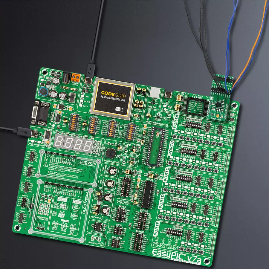
Development board
EasyPIC v7a is the seventh generation of PIC development boards specially designed for the needs of rapid development of embedded applications. It supports a wide range of 8-bit PIC microcontrollers from Microchip and has a broad set of unique functions, such as the first-ever embedded debugger/programmer over USB-C. The development board is well organized and designed so that the end-user has all the necessary elements in one place, such as switches, buttons, indicators, connectors, and others. With four different connectors for each port, EasyPIC v7a allows you to connect accessory boards, sensors, and custom electronics more efficiently than ever. Each part of the EasyPIC v7a development board
contains the components necessary for the most efficient operation of the same board. In addition to the advanced integrated CODEGRIP programmer/debugger module, which offers many valuable programming/debugging options and seamless integration with the Mikroe software environment, the board also includes a clean and regulated power supply module for the development board. It can use various external power sources, including an external 12V power supply, 7-23V AC or 9-32V DC via DC connector/screw terminals, and a power source via the USB Type-C (USB-C) connector. Communication options such as USB-UART and RS-232 are also included, alongside the well-
established mikroBUS™ standard, three display options (7-segment, graphical, and character-based LCD), and several different DIP sockets. These sockets cover a wide range of 8-bit PIC MCUs, from PIC10F, PIC12F, PIC16F, PIC16Enh, PIC18F, PIC18FJ, and PIC18FK families. EasyPIC v7a is an integral part of the Mikroe ecosystem for rapid development. Natively supported by Mikroe software tools, it covers many aspects of prototyping and development thanks to a considerable number of different Click boards™ (over a thousand boards), the number of which is growing every day.

Microcontroller Overview
MCU Card / MCU
Architecture
PIC
MCU Memory (KB)
64
Silicon Vendor
Microchip
Pin count
28
RAM (Bytes)
3896
Used MCU Pins
mikroBUS™ mapper
Take a closer look
Click board™ Schematic
Step by step
Project assembly

Start by selecting your development board and Click board™. Begin with the EasyPIC v7a as your development board.


Track your results in real time
Application Output
1. Application Output - In Debug mode, the 'Application Output' window enables real-time data monitoring, offering direct insight into execution results. Ensure proper data display by configuring the environment correctly using the provided tutorial.

2. UART Terminal - Use the UART Terminal to monitor data transmission via a USB to UART converter, allowing direct communication between the Click board™ and your development system. Configure the baud rate and other serial settings according to your project's requirements to ensure proper functionality. For step-by-step setup instructions, refer to the provided tutorial.

3. Plot Output - The Plot feature offers a powerful way to visualize real-time sensor data, enabling trend analysis, debugging, and comparison of multiple data points. To set it up correctly, follow the provided tutorial, which includes a step-by-step example of using the Plot feature to display Click board™ readings. To use the Plot feature in your code, use the function: plot(*insert_graph_name*, variable_name);. This is a general format, and it is up to the user to replace 'insert_graph_name' with the actual graph name and 'variable_name' with the parameter to be displayed.

Software Support
Library Description
This library contains API for PIXI Click driver.
Key functions:
pixi_write_reg- Generic write functionpixi_read_reg- Generic read function
Open Source
Code example
The complete application code and a ready-to-use project are available through the NECTO Studio Package Manager for direct installation in the NECTO Studio. The application code can also be found on the MIKROE GitHub account.
/*!
 * \file
 * \brief Pixi Click example
 *
 * # Description
 * This example showcases how to initialize, configure and use the Pixi Click moduel. The Click
 * features Maxim Integrated's versatile, proprietary PIXI™ technology - the industry's first
 * configurable 20-channel mixed-signal data converter.
 *
 * The demo application is composed of two sections :
 *
 * ## Application Init
 * This function initializes and configures the Click and logger modules. After the initial setup
 * a device id check is performed which will stop the module if the check fails. Additional con-
 * figurating is done in the default_cfg(...) function.
 *
 * ## Application Task
 * This function sets the output signal on port 0 to different values every second.
 *
 * \author MikroE Team
 *
 */
// ------------------------------------------------------------------- INCLUDES

#include "board.h"
#include "log.h"
#include "pixi.h"

// ------------------------------------------------------------------ VARIABLES

static pixi_t pixi;
static log_t logger;

// ------------------------------------------------------ APPLICATION FUNCTIONS

void application_init ( )
{
    log_cfg_t log_cfg;
    pixi_cfg_t cfg;
    uint32_t res;

    /**
     * Logger initialization.
     * Default baud rate: 115200
     * Default log level: LOG_LEVEL_DEBUG
     * @note If USB_UART_RX and USB_UART_TX
     * are defined as HAL_PIN_NC, you will
     * need to define them manually for log to work.
     * See @b LOG_MAP_USB_UART macro definition for detailed explanation.
     */
    LOG_MAP_USB_UART( log_cfg );
    log_init( &logger, &log_cfg );
    log_info( &logger, "---- Application Init ----" );
    Delay_ms ( 100 );

    //  Click initialization.

    pixi_cfg_setup( &cfg );
    PIXI_MAP_MIKROBUS( cfg, MIKROBUS_1 );
    pixi_init( &pixi, &cfg );

    //  Device ID check.

    pixi_read_reg( &pixi, PIXI_REG_DEVICE_ID, &res );
    if ( res != 1060 )
    {
        log_printf( &logger, "ERROR : WRONG DEVICE ID!\r\n" );
        for( ; ; );
    }
    else
    {
        log_printf( &logger, "Driver Init - DONE!\r\n" );
    }

    //  Default configuration.

    pixi_default_cfg( &pixi );
}

void application_task ( )
{
    pixi_write_reg( &pixi, PIXI_REG_GPO_DATA, 0x1 );
    log_printf( &logger, "Led on\r\n" );
    Delay_ms ( 1000 );
    Delay_ms ( 1000 );
    pixi_write_reg( &pixi, PIXI_REG_GPO_DATA, 0 );
    log_printf( &logger, "Led off\r\n" );
    Delay_ms ( 1000 );
    Delay_ms ( 1000 );
}

int main ( void )
{
    /* Do not remove this line or clock might not be set correctly. */
    #ifdef PREINIT_SUPPORTED
    preinit();
    #endif

    application_init( );

    for ( ; ; )
    {
        application_task( );
    }

    return 0;
}

// ------------------------------------------------------------------------ END