Achieve seamless signal conversion with MAX22000 and PIC18F57Q43
ADC + DAC in perfect harmony
Published Feb 13, 2024
Click board™
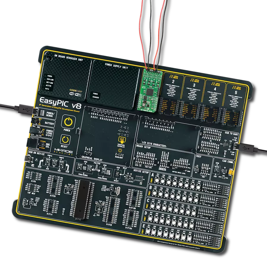
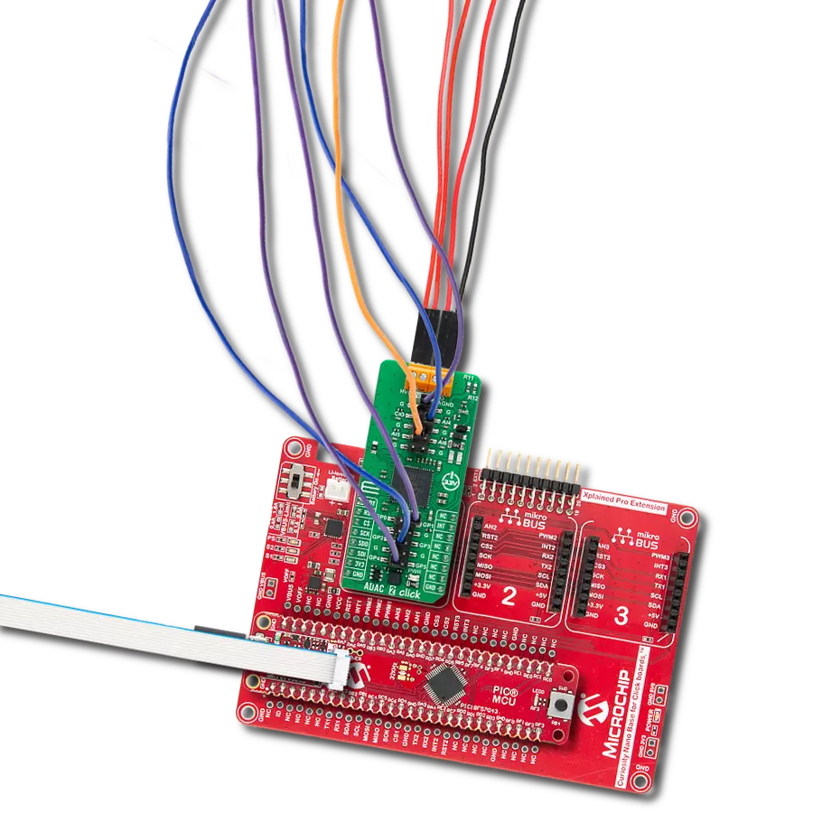
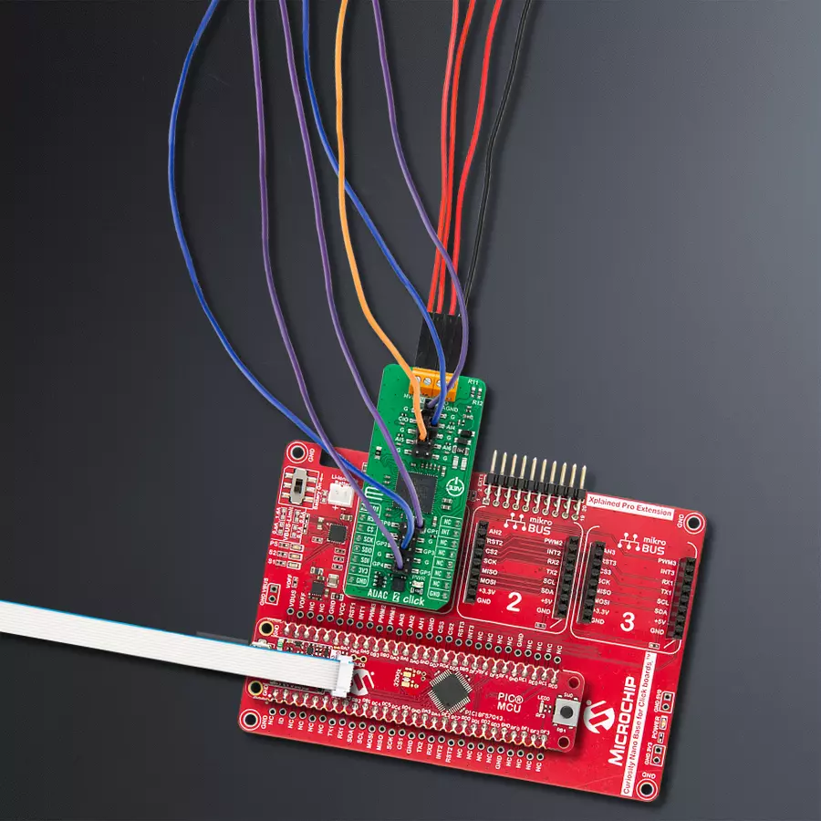
ADAC 2 Click
Dev. board
Curiosity Nano with PIC18F57Q43
Compiler
NECTO Studio
MCU
PIC18F57Q43
The complete package for applications that necessitate combined ADC and DAC operation
A
A
Hardware Overview
How does it work?
ADAC 2 Click is based on the MAX22000, an industrial-grade, software-configurable analog input/output solution from Analog Devices. It provides a high-performance 18-bit DAC in the transmit path and a 24-bit delta-sigma ADC in the receive path. The transmit path (analog output) and the receive path (analog inputs) are entirely independent; thus, they can be programmed for different configurations and modes of operation. Thanks to its outstanding performance and features, this board is designed to support various industrial applications such as programmable logic controllers (PLCs), programmable automation controllers (PACs), and process control applications that require configurable analog I/O. This Click board™ communicates with an MCU through a standard SPI interface for all configuration and management information with a maximum frequency of 20MHz. The MAX22000 provides multiple voltages and current ranges for its inputs and outputs to maintain the best accuracy. It sets the linear range at 105% of the nominal range and the full scale at 125% of the nominal range.
For example, for a ±10V nominal range, the MAX22000 provides a linear range of ±10.5V and a full-scale range of ±12.5V. Other ranges can be achieved by configuring the appropriate registers. The MAX22000 also offers one output marked as CIO, configured as voltage or current output, alongside three analog inputs (AI4, AI5, and AI6) configurable as voltage or current inputs. Besides their use as general-purpose analog inputs, the AI5 and AI6 pins can also be configured as a differential programmable gain amplifier (PGA) for either low-voltage or high-voltage inputs to support RTD and thermocouple measurements. A high-performance filter allows the ADC to provide 50Hz/60Hz normal mode rejection at selected ADC data rates. Current measurement using the AI5 and AI6 pins relies on an external precision resistor to perform the current-to-voltage conversion. A GPIO pin on the additional GPIO header can control an external analog switch to connect or disconnect the current sense resistor electronically for current measurements that do not use a differential sensor.
In addition, several mikroBUS™ pins are used. An active-low reset signal routed on the RST pin of the mikroBUS™ socket activates a hardware reset of the system (all registers go to their power-on default states, analog output goes high impedance, analog inputs power down, and ADC conversion stops) while the INT pin on the mikroBUS™ socket represents a standard interrupt feature providing a user with feedback information. It also has an additional data-ready interrupt marked as RDY and routed on the AN pin of the mikroBUS™ socket, used to signal when a new ADC conversion result is available in the data register. This Click board™ can only be operated with a 3.3V logic voltage level. The board must perform appropriate logic voltage level conversion before using MCUs with different logic levels. However, the Click board™ comes equipped with a library containing functions and an example code that can be used as a reference for further development.

Features overview
Development board
PIC18F57Q43 Curiosity Nano evaluation kit is a cutting-edge hardware platform designed to evaluate microcontrollers within the PIC18-Q43 family. Central to its design is the inclusion of the powerful PIC18F57Q43 microcontroller (MCU), offering advanced functionalities and robust performance. Key features of this evaluation kit include a yellow user LED and a responsive
mechanical user switch, providing seamless interaction and testing. The provision for a 32.768kHz crystal footprint ensures precision timing capabilities. With an onboard debugger boasting a green power and status LED, programming and debugging become intuitive and efficient. Further enhancing its utility is the Virtual serial port (CDC) and a debug GPIO channel (DGI
GPIO), offering extensive connectivity options. Powered via USB, this kit boasts an adjustable target voltage feature facilitated by the MIC5353 LDO regulator, ensuring stable operation with an output voltage ranging from 1.8V to 5.1V, with a maximum output current of 500mA, subject to ambient temperature and voltage constraints.

Microcontroller Overview
MCU Card / MCU

Architecture
PIC
MCU Memory (KB)
128
Silicon Vendor
Microchip
Pin count
48
RAM (Bytes)
8196
You complete me!
Accessories
Curiosity Nano Base for Click boards is a versatile hardware extension platform created to streamline the integration between Curiosity Nano kits and extension boards, tailored explicitly for the mikroBUS™-standardized Click boards and Xplained Pro extension boards. This innovative base board (shield) offers seamless connectivity and expansion possibilities, simplifying experimentation and development. Key features include USB power compatibility from the Curiosity Nano kit, alongside an alternative external power input option for enhanced flexibility. The onboard Li-Ion/LiPo charger and management circuit ensure smooth operation for battery-powered applications, simplifying usage and management. Moreover, the base incorporates a fixed 3.3V PSU dedicated to target and mikroBUS™ power rails, alongside a fixed 5.0V boost converter catering to 5V power rails of mikroBUS™ sockets, providing stable power delivery for various connected devices.

Used MCU Pins
mikroBUS™ mapper
Take a closer look
Click board™ Schematic

Step by step
Project assembly

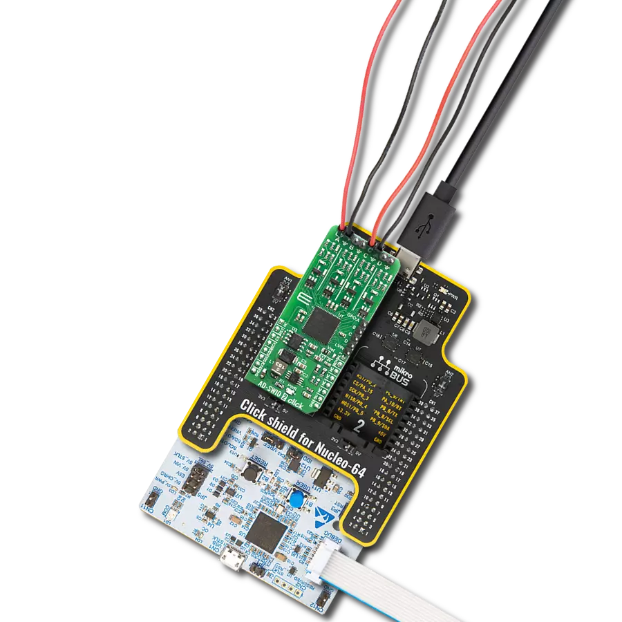
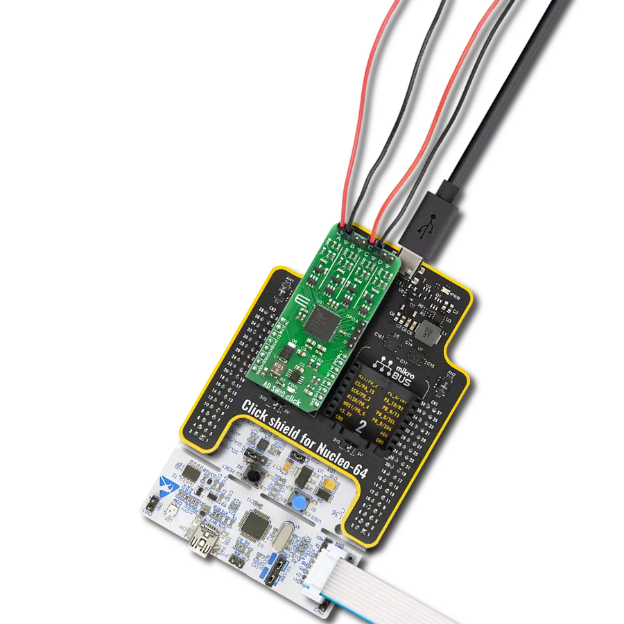
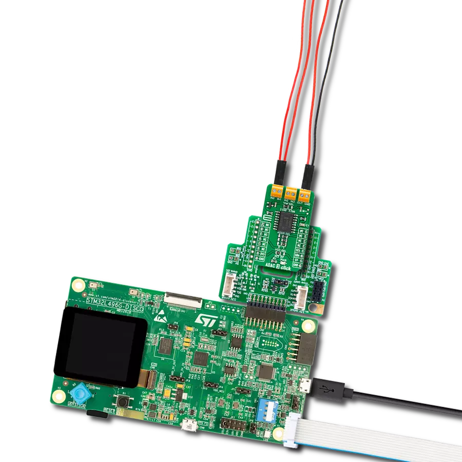
Start by selecting your development board and Click board™. Begin with the Curiosity Nano with PIC18F57Q43 as your development board.


Track your results in real time
Application Output
1. Application Output - In Debug mode, the 'Application Output' window enables real-time data monitoring, offering direct insight into execution results. Ensure proper data display by configuring the environment correctly using the provided tutorial.

2. UART Terminal - Use the UART Terminal to monitor data transmission via a USB to UART converter, allowing direct communication between the Click board™ and your development system. Configure the baud rate and other serial settings according to your project's requirements to ensure proper functionality. For step-by-step setup instructions, refer to the provided tutorial.

3. Plot Output - The Plot feature offers a powerful way to visualize real-time sensor data, enabling trend analysis, debugging, and comparison of multiple data points. To set it up correctly, follow the provided tutorial, which includes a step-by-step example of using the Plot feature to display Click board™ readings. To use the Plot feature in your code, use the function: plot(*insert_graph_name*, variable_name);. This is a general format, and it is up to the user to replace 'insert_graph_name' with the actual graph name and 'variable_name' with the parameter to be displayed.

Software Support
Library Description
This library contains API for ADAC 2 Click driver.
Key functions:
adac2_set_active_ain_channelThis function sets the active analog input channel.adac2_read_voltageThis function reads the RAW ADC value of the previous conversion and converts it to voltage.adac2_write_dacThis function sets the analog output by writing to the AO_DATA_WR register.
Open Source
Code example
The complete application code and a ready-to-use project are available through the NECTO Studio Package Manager for direct installation in the NECTO Studio. The application code can also be found on the MIKROE GitHub account.
/*!
 * @file main.c
 * @brief ADAC 2 Click example
 *
 * # Description
 * This example demonstrates the use of ADAC 2 Click board by setting the DAC output (CIO)
 * and reading the ADC results from a single-ended channel (AI4) and from a differential
 * channel (AI5+, AI6-) as well as toggling all GPIO pins.
 *
 * The demo application is composed of two sections :
 *
 * ## Application Init
 * Initializes the driver and performs the Click default configuration which enables
 * DAC voltage output, sets the analog input mode to single-ended for AI4 and
 * differential (AI5+, AI6-), and enables all GPIOs as output.
 *
 * ## Application Task
 * Reads the ADC results from a single-ended (AI4) and a differential (AI5+, AI6-) channels,
 * then sets the raw DAC output increasing the value by 10000 after each iteration, and toggles
 * all GPIO pins. The results will be displayed on the USB UART approximately once per second.
 *
 * @author Stefan Filipovic
 *
 */

#include "board.h"
#include "log.h"
#include "adac2.h"

static adac2_t adac2;
static log_t logger;

void application_init ( void )
{
    log_cfg_t log_cfg;  /**< Logger config object. */
    adac2_cfg_t adac2_cfg;  /**< Click config object. */

    /**
     * Logger initialization.
     * Default baud rate: 115200
     * Default log level: LOG_LEVEL_DEBUG
     * @note If USB_UART_RX and USB_UART_TX
     * are defined as HAL_PIN_NC, you will
     * need to define them manually for log to work.
     * See @b LOG_MAP_USB_UART macro definition for detailed explanation.
     */
    LOG_MAP_USB_UART( log_cfg );
    log_init( &logger, &log_cfg );
    log_info( &logger, " Application Init " );

    // Click initialization.
    adac2_cfg_setup( &adac2_cfg );
    ADAC2_MAP_MIKROBUS( adac2_cfg, MIKROBUS_1 );
    if ( SPI_MASTER_ERROR == adac2_init( &adac2, &adac2_cfg ) )
    {
        log_error( &logger, " Communication init." );
        for ( ; ; );
    }

    if ( ADAC2_ERROR == adac2_default_cfg ( &adac2 ) )
    {
        log_error( &logger, " Default configuration." );
        for ( ; ; );
    }

    log_info( &logger, " Application Task " );
}

void application_task ( void )
{
    float voltage;
    if ( ADAC2_OK == adac2_set_active_ain_channel ( &adac2, ADAC2_CH_AI4_SINGLE_ENDED ) )
    {
        adac2_start_conversion ( &adac2, ADAC2_DATA_RATE_450_SPS );
        // Waits for the availability of the conversion result
        while ( adac2_get_rdy_pin ( &adac2 ) );
        adac2_stop_conversion ( &adac2 );
        if ( ADAC2_OK == adac2_read_voltage ( &adac2, ADAC2_FULL_SCALE_RANGE_12p5V, &voltage ) )
        {
            log_printf ( &logger, " Channel AI4 single-ended: %.2f V\r\n", voltage );
        }
    }
    if ( ADAC2_OK == adac2_set_active_ain_channel ( &adac2, ADAC2_CH_AI5_AI6_DIFFERENTIAL_25V ) )
    {
        adac2_start_conversion ( &adac2, ADAC2_DATA_RATE_450_SPS );
        // Waits for the availability of the conversion result
        while ( adac2_get_rdy_pin ( &adac2 ) );
        adac2_stop_conversion ( &adac2 );
        if ( ADAC2_OK == adac2_read_voltage ( &adac2, ADAC2_FULL_SCALE_RANGE_25V, &voltage ) )
        {
            log_printf ( &logger, " Channel AI5-AI6 differential: %.2f V\r\n", voltage );
        }
    }

    static int32_t dac = ADAC2_DAC_MIN_VALUE;
    if ( ADAC2_OK == adac2_write_dac ( &adac2, dac ) )
    {
        log_printf ( &logger, " DAC: %ld\r\n", dac );
        dac += 5000;
        if ( dac > ADAC2_DAC_MAX_VALUE )
        {
            dac = ADAC2_DAC_MIN_VALUE;
        }
    }

    uint32_t gpio_data;
    if ( ADAC2_OK == adac2_read_register ( &adac2, ADAC2_REG_GEN_GPIO_CTRL, &gpio_data ) )
    {
        gpio_data ^= ADAC2_GPIO_ALL_MASK;
        if ( ADAC2_OK == adac2_write_register ( &adac2, ADAC2_REG_GEN_GPIO_CTRL, gpio_data ) )
        {
            log_printf ( &logger, " GPIO: 0x%.2X\r\n\n", ( uint16_t ) ( gpio_data & ADAC2_GPIO_ALL_MASK ) );
        }
    }
    Delay_ms ( 1000 );
}

int main ( void )
{
    /* Do not remove this line or clock might not be set correctly. */
    #ifdef PREINIT_SUPPORTED
    preinit();
    #endif

    application_init( );

    for ( ; ; )
    {
        application_task( );
    }

    return 0;
}

// ------------------------------------------------------------------------ END
Additional Support
Resources
Category:ADC-DAC