Convert your signals simultaneously using PCF8591 and PIC18F57Q43
ADC/DAC combo

Published Feb 13, 2024
Click board™
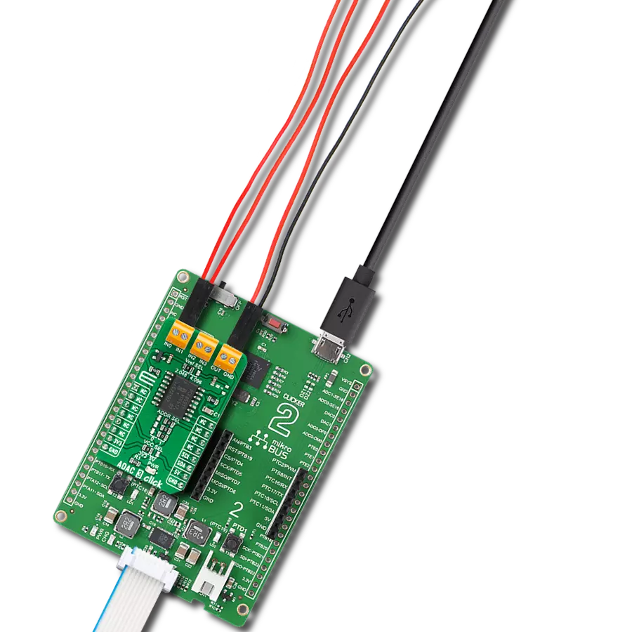
ADAC 3 Click
Dev. board
Curiosity Nano with PIC18F57Q43
Compiler
NECTO Studio
MCU
PIC18F57Q43
High-performance data acquisition solution
A
A
Hardware Overview
How does it work?
ADAC 3 Click is based on the PCF8591, a low-power CMOS data acquisition device from NXP Semiconductors. The PCF8591 comes with four analog inputs configurable as single-ended or differential inputs used to measure voltages, alongside one analog output representing an 8-bit digital-to-analog converter. In addition to measuring voltage, the user can create them as desired and even use DAC and ADC together to generate an input to a circuit and measure the results with the ADC, making it suitable for various control, monitoring, or measurement applications. By its internal structure, the PCF8591 also consists of
an analog input multiplexing circuit and an on-chip track and hold function alongside a serial interface block. This Click board™ communicates with MCU using the standard I2C 2-Wire interface with a maximum clock frequency of 100kHz. The PCF8591 has a 7-bit slave address with the first four MSBs fixed to 1001. The address pins A0, A1, and A2 are programmed by the user and determine the value of the last three LSBs of the slave address, which can be selected by positioning onboard SMD jumpers labeled as ADDR SEL to an appropriate position marked as 0 or 1. Besides, the user can choose the PCF8591
reference voltage value by positioning the SMD jumper labeled VREF SEL, choosing between 2,048 and 4,096V provided by MAX6104 and MAX6106. This Click board™ can operate with either 3.3V or 5V logic voltage levels selected via the VCC SEL jumper. This way, both 3.3V and 5V capable MCUs can use the communication lines properly. However, the Click board™ comes equipped with a library containing easy-to-use functions and an example code that can be used, as a reference, for further development.

Features overview
Development board
PIC18F57Q43 Curiosity Nano evaluation kit is a cutting-edge hardware platform designed to evaluate microcontrollers within the PIC18-Q43 family. Central to its design is the inclusion of the powerful PIC18F57Q43 microcontroller (MCU), offering advanced functionalities and robust performance. Key features of this evaluation kit include a yellow user LED and a responsive
mechanical user switch, providing seamless interaction and testing. The provision for a 32.768kHz crystal footprint ensures precision timing capabilities. With an onboard debugger boasting a green power and status LED, programming and debugging become intuitive and efficient. Further enhancing its utility is the Virtual serial port (CDC) and a debug GPIO channel (DGI
GPIO), offering extensive connectivity options. Powered via USB, this kit boasts an adjustable target voltage feature facilitated by the MIC5353 LDO regulator, ensuring stable operation with an output voltage ranging from 1.8V to 5.1V, with a maximum output current of 500mA, subject to ambient temperature and voltage constraints.

Microcontroller Overview
MCU Card / MCU

Architecture
PIC
MCU Memory (KB)
128
Silicon Vendor
Microchip
Pin count
48
RAM (Bytes)
8196
You complete me!
Accessories
Curiosity Nano Base for Click boards is a versatile hardware extension platform created to streamline the integration between Curiosity Nano kits and extension boards, tailored explicitly for the mikroBUS™-standardized Click boards and Xplained Pro extension boards. This innovative base board (shield) offers seamless connectivity and expansion possibilities, simplifying experimentation and development. Key features include USB power compatibility from the Curiosity Nano kit, alongside an alternative external power input option for enhanced flexibility. The onboard Li-Ion/LiPo charger and management circuit ensure smooth operation for battery-powered applications, simplifying usage and management. Moreover, the base incorporates a fixed 3.3V PSU dedicated to target and mikroBUS™ power rails, alongside a fixed 5.0V boost converter catering to 5V power rails of mikroBUS™ sockets, providing stable power delivery for various connected devices.

Used MCU Pins
mikroBUS™ mapper
Take a closer look
Click board™ Schematic

Step by step
Project assembly

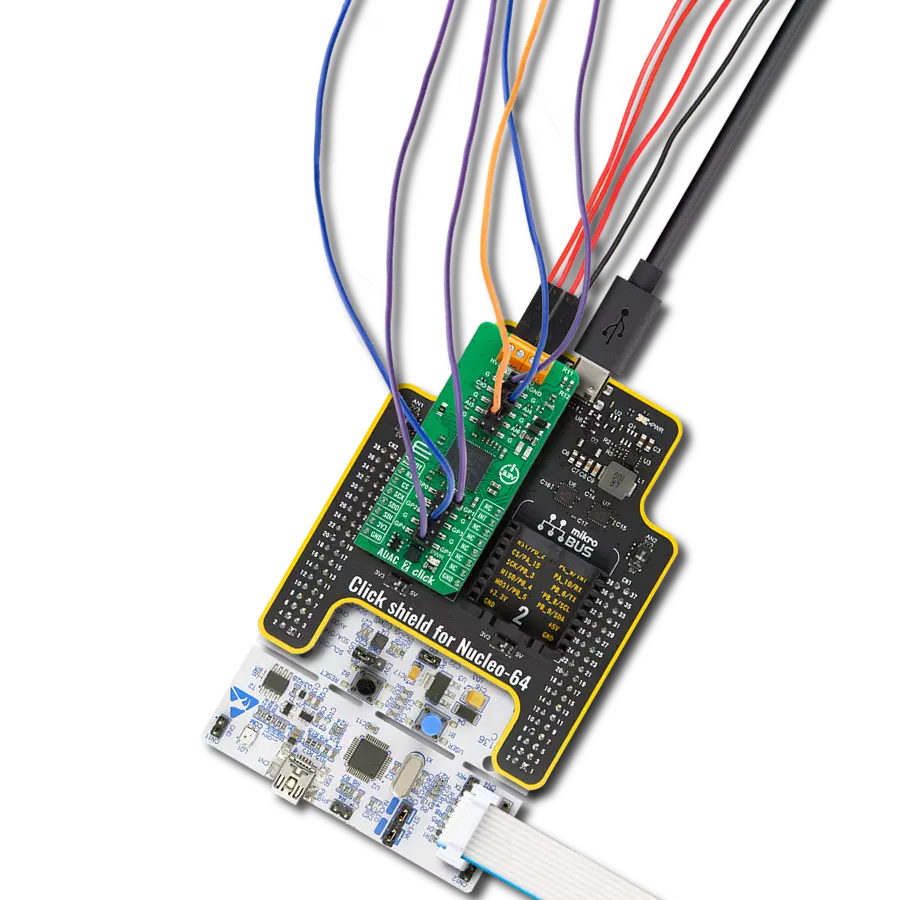
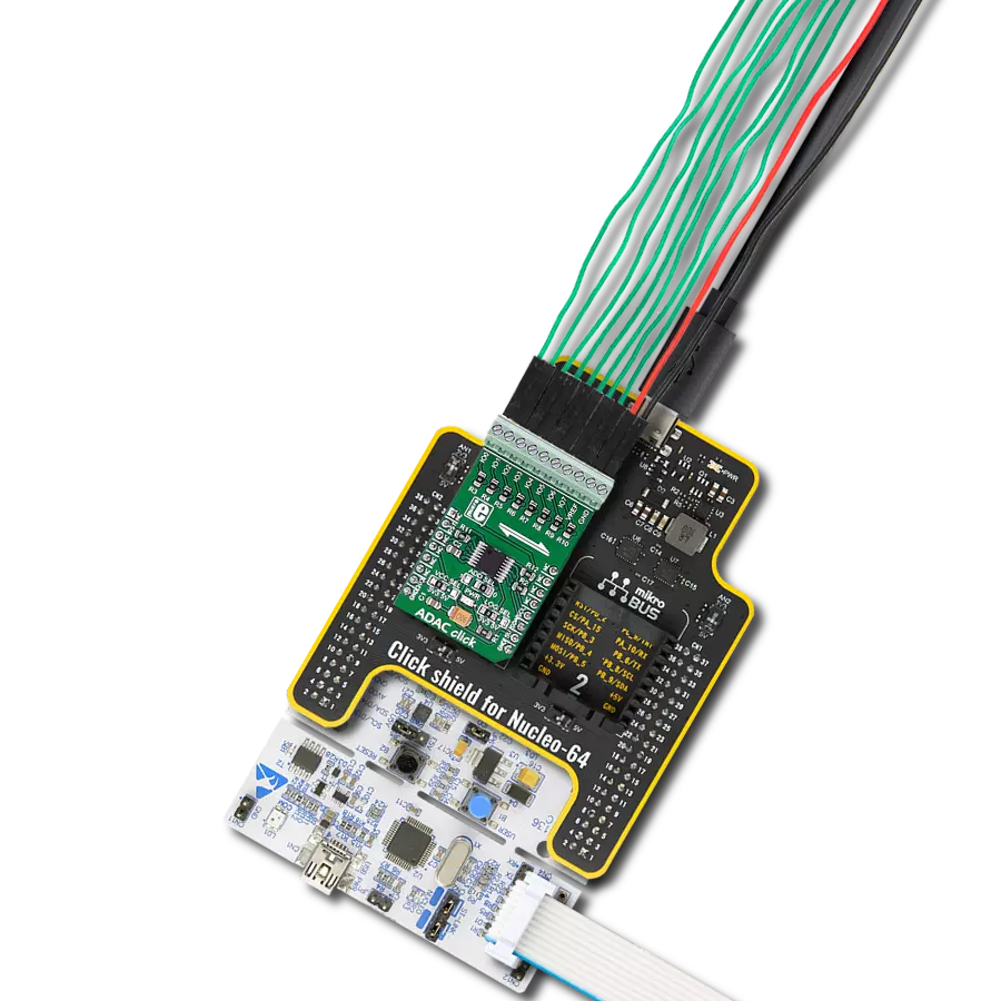
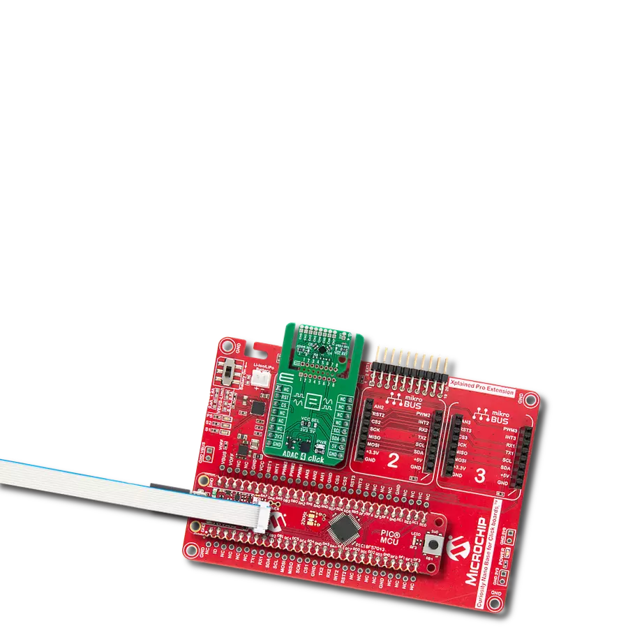
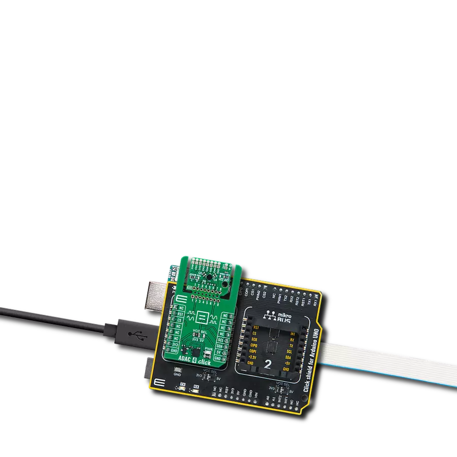
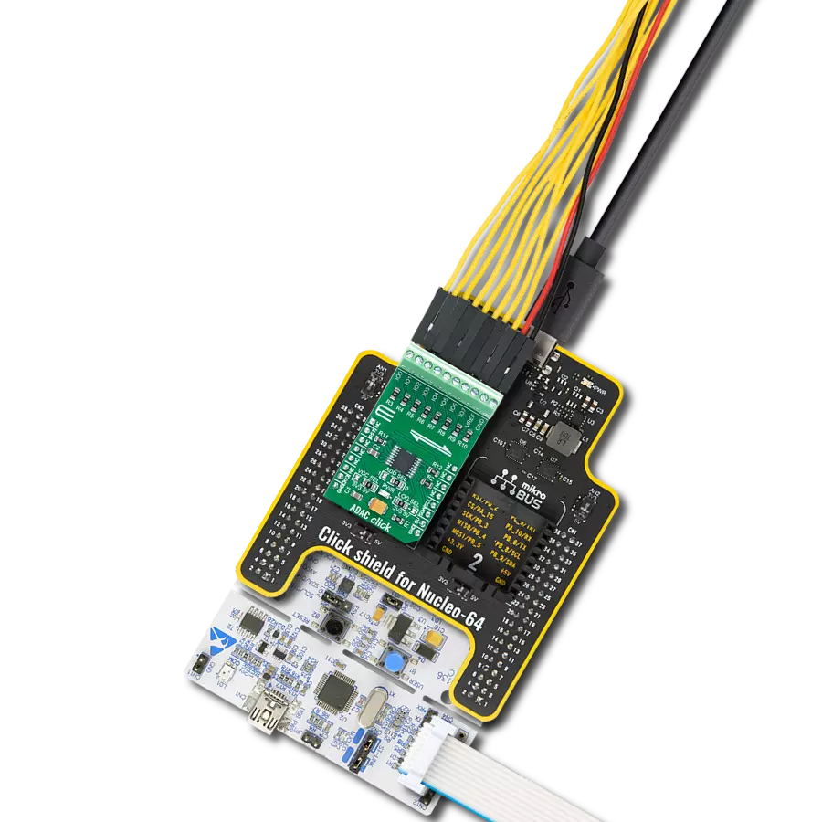
Start by selecting your development board and Click board™. Begin with the Curiosity Nano with PIC18F57Q43 as your development board.


Software Support
Library Description
This library contains API for ADAC 3 Click driver.
Key functions:
adac3_write_controlThis function writes a control byte by using I2C serial interface.adac3_write_dacThis function writes a DAC byte by using I2C serial interface.adac3_read_adcThis function reads the AD conversion byte by using I2C serial interface.
Open Source
Code example
The complete application code and a ready-to-use project are available through the NECTO Studio Package Manager for direct installation in the NECTO Studio. The application code can also be found on the MIKROE GitHub account.
/*!
 * @file main.c
 * @brief ADAC3 Click example
 *
 * # Description
 * This example demonstrates the use of ADAC 3 Click board by setting the DAC output
 * and reading the ADC results from 2 single-ended channels (AIN0, AIN1) and from a
 * differential channel (AIN2+, AIN3-).
 *
 * The demo application is composed of two sections :
 *
 * ## Application Init
 * Initializes the driver and performs the Click default configuration which enables
 * DAC output, sets the analog input mode to single-ended (AIN0, AIN1) and
 * differential (AIN2+, AIN3-), and enables the auto increment mode.
 *
 * ## Application Task
 * Sets the DAC output increasing the value by 1 after each iteration, and reads the
 * ADC results from 2 single-ended and 1 differential channels, and displays the results
 * on the USB UART every 100ms approximately.
 *
 * @note
 * Inputs should be connected to GND when not in use.
 *
 * @author Stefan Filipovic
 *
 */

#include "board.h"
#include "log.h"
#include "adac3.h"

static adac3_t adac3;
static log_t logger;

void application_init ( void )
{
    log_cfg_t log_cfg;  /**< Logger config object. */
    adac3_cfg_t adac3_cfg;  /**< Click config object. */

    /**
     * Logger initialization.
     * Default baud rate: 115200
     * Default log level: LOG_LEVEL_DEBUG
     * @note If USB_UART_RX and USB_UART_TX
     * are defined as HAL_PIN_NC, you will
     * need to define them manually for log to work.
     * See @b LOG_MAP_USB_UART macro definition for detailed explanation.
     */
    LOG_MAP_USB_UART( log_cfg );
    log_init( &logger, &log_cfg );
    log_info( &logger, " Application Init " );

    // Click initialization.
    adac3_cfg_setup( &adac3_cfg );
    ADAC3_MAP_MIKROBUS( adac3_cfg, MIKROBUS_1 );
    if ( I2C_MASTER_ERROR == adac3_init( &adac3, &adac3_cfg ) )
    {
        log_error( &logger, " Communication init." );
        for ( ; ; );
    }

    if ( ADAC3_ERROR == adac3_default_cfg ( &adac3 ) )
    {
        log_error( &logger, " Default configuration." );
        for ( ; ; );
    }

    log_info( &logger, " Application Task " );
}

void application_task ( void )
{
    static uint8_t dac = 0;
    uint8_t ain0, ain1, ain2_ain3_diff;
    if ( ADAC3_OK == adac3_write_dac ( &adac3, dac ) )
    {
        log_printf ( &logger, " DAC : %u mV\r\n",
                     ( uint16_t ) ( ( ADAC3_VREF_2048mV / ADAC3_RESOLUTION ) * dac++ ) );
    }
    if ( ADAC3_OK == adac3_read_adc ( &adac3, &ain0 ) )
    {
        log_printf ( &logger, " AIN0+: %u mV\r\n",
                     ( uint16_t ) ( ( ADAC3_VREF_2048mV / ADAC3_RESOLUTION ) * ain0 ) );
    }
    if ( ADAC3_OK == adac3_read_adc ( &adac3, &ain1 ) )
    {
        log_printf ( &logger, " AIN1+: %u mV\r\n",
                     ( uint16_t ) ( ( ADAC3_VREF_2048mV / ADAC3_RESOLUTION ) * ain1 ) );
    }
    if ( ADAC3_OK == adac3_read_adc ( &adac3, &ain2_ain3_diff ) )
    {
        log_printf ( &logger, " AIN2+ - AIN3-: %d mV\r\n\n",
                     ( int16_t ) ( ( ADAC3_VREF_2048mV / ADAC3_RESOLUTION ) * ( int8_t ) ain2_ain3_diff ) );
    }
    Delay_ms ( 100 );
}

int main ( void )
{
    /* Do not remove this line or clock might not be set correctly. */
    #ifdef PREINIT_SUPPORTED
    preinit();
    #endif

    application_init( );

    for ( ; ; )
    {
        application_task( );
    }

    return 0;
}

// ------------------------------------------------------------------------ END
Additional Support
Resources
Category:ADC-DAC