Upgrade data acquisition process with MCP3428 and PIC18F57Q43
Unleash your data's true potential

Published Feb 13, 2024
Click board™
ADC 3 Click
Dev. board
Curiosity Nano with PIC18F57Q43
Compiler
NECTO Studio
MCU
PIC18F57Q43
Achieve unparalleled data accuracy in your designs with our top-of-the-line ADC
A
A
Hardware Overview
How does it work?
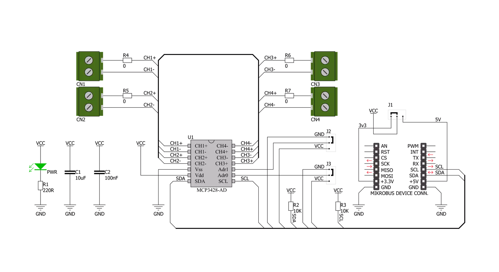
ADC 3 Click is based on the MCP3428, a differential multi-channel low-power, 16-bit ΔΣ A/D converter from Microchip. The MCP3428 contains an input channel selection multiplexer (CH1, CH2, CH3, or CH4), an onboard voltage reference, and an internal oscillator. It performs conversions at rates of 15, 60, or 240 samples per second (12, 14, or 16 bits), depending on user-controllable configuration bit settings, and has a programmable gain amplifier (x1, x2, x4, or x8) which makes it an ideal choice for monitoring extremely low-voltage sensors. All four channels have differential inputs monitoring a full-scale range of 4.096VDC or ±2.048V differentially. The MCP3428 has two conversion modes: Continuous and One-Shot mode. In the Continuous
Conversion mode, the ADC converts the inputs continuously, while in the One-Shot Conversion mode, the MCP3428 converts the input once and stays in the low-power Standby mode until it receives another command for a new conversion. The standby mode reduces current consumption significantly during idle periods. This ADDC can be used for various high-accuracy analog-to-digital data conversion applications where ease of use and low power consumption are significant considerations. ADC 3 Click communicates with an MCU using the standard I2C 2-Wire interface to read data and configure settings, supporting High-Speed Mode up to 3.4MHz. It also has a 7-bit slave address with the first four MSBs fixed to 1101. The address pins, ADR0 and ADR1, are
programmed by the user and determine the value of the last three LSBs of the slave address, allowing up to 8 devices to operate on the same bus segment. The value of these address pins can be set by positioning onboard SMD jumpers labeled as I2C ADR to an appropriate position marked as 0 or 1. This Click board™ can operate with both 3.3V and 5V logic voltage levels selected via the PWR SEL jumper. This way, it is allowed for both 3.3V and 5V capable MCUs to use the communication lines properly. However, the Click board™ comes equipped with a library containing easy-to-use functions and an example code that can be used, as a reference, for further development.

Features overview
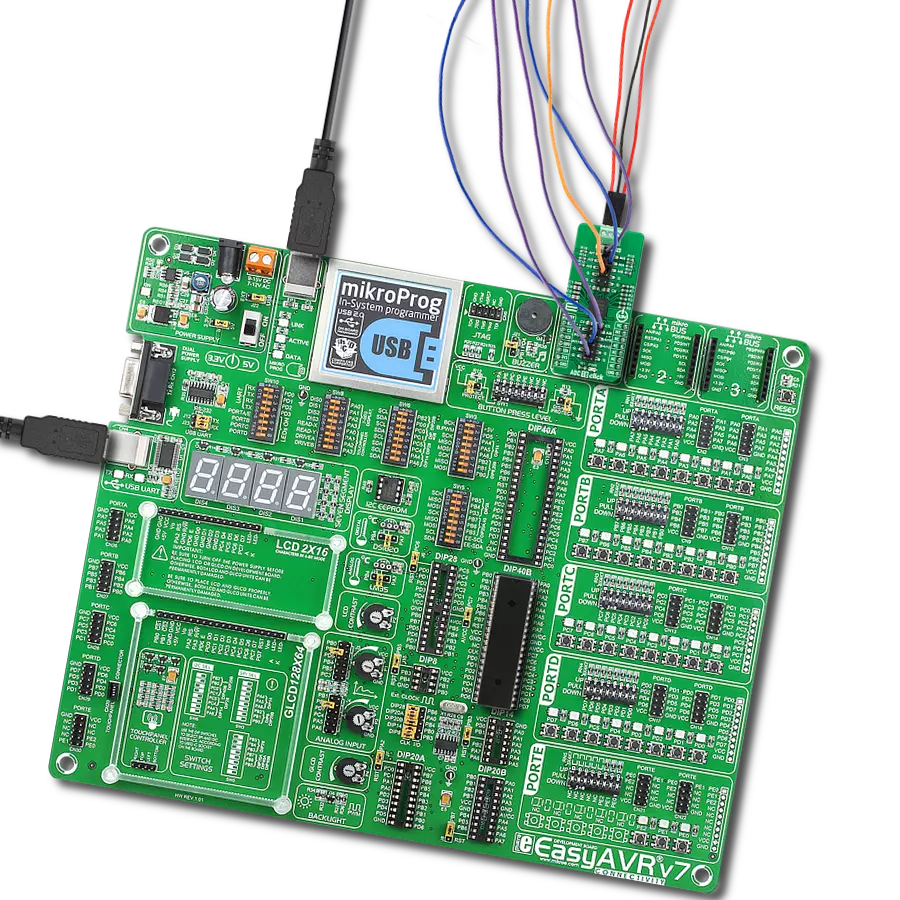
Development board
PIC18F57Q43 Curiosity Nano evaluation kit is a cutting-edge hardware platform designed to evaluate microcontrollers within the PIC18-Q43 family. Central to its design is the inclusion of the powerful PIC18F57Q43 microcontroller (MCU), offering advanced functionalities and robust performance. Key features of this evaluation kit include a yellow user LED and a responsive
mechanical user switch, providing seamless interaction and testing. The provision for a 32.768kHz crystal footprint ensures precision timing capabilities. With an onboard debugger boasting a green power and status LED, programming and debugging become intuitive and efficient. Further enhancing its utility is the Virtual serial port (CDC) and a debug GPIO channel (DGI
GPIO), offering extensive connectivity options. Powered via USB, this kit boasts an adjustable target voltage feature facilitated by the MIC5353 LDO regulator, ensuring stable operation with an output voltage ranging from 1.8V to 5.1V, with a maximum output current of 500mA, subject to ambient temperature and voltage constraints.

Microcontroller Overview
MCU Card / MCU

Architecture
PIC
MCU Memory (KB)
128
Silicon Vendor
Microchip
Pin count
48
RAM (Bytes)
8196
You complete me!
Accessories
Curiosity Nano Base for Click boards is a versatile hardware extension platform created to streamline the integration between Curiosity Nano kits and extension boards, tailored explicitly for the mikroBUS™-standardized Click boards and Xplained Pro extension boards. This innovative base board (shield) offers seamless connectivity and expansion possibilities, simplifying experimentation and development. Key features include USB power compatibility from the Curiosity Nano kit, alongside an alternative external power input option for enhanced flexibility. The onboard Li-Ion/LiPo charger and management circuit ensure smooth operation for battery-powered applications, simplifying usage and management. Moreover, the base incorporates a fixed 3.3V PSU dedicated to target and mikroBUS™ power rails, alongside a fixed 5.0V boost converter catering to 5V power rails of mikroBUS™ sockets, providing stable power delivery for various connected devices.

Used MCU Pins
mikroBUS™ mapper
Take a closer look
Click board™ Schematic
Step by step
Project assembly

Start by selecting your development board and Click board™. Begin with the Curiosity Nano with PIC18F57Q43 as your development board.


Track your results in real time
Application Output
1. Application Output - In Debug mode, the 'Application Output' window enables real-time data monitoring, offering direct insight into execution results. Ensure proper data display by configuring the environment correctly using the provided tutorial.

2. UART Terminal - Use the UART Terminal to monitor data transmission via a USB to UART converter, allowing direct communication between the Click board™ and your development system. Configure the baud rate and other serial settings according to your project's requirements to ensure proper functionality. For step-by-step setup instructions, refer to the provided tutorial.

3. Plot Output - The Plot feature offers a powerful way to visualize real-time sensor data, enabling trend analysis, debugging, and comparison of multiple data points. To set it up correctly, follow the provided tutorial, which includes a step-by-step example of using the Plot feature to display Click board™ readings. To use the Plot feature in your code, use the function: plot(*insert_graph_name*, variable_name);. This is a general format, and it is up to the user to replace 'insert_graph_name' with the actual graph name and 'variable_name' with the parameter to be displayed.

Software Support
Library Description
This library contains API for ADC 3 Click driver.
Key functions:
adc3_default_cfg- This function is used to initiate general call reset.adc3_read_voltage- This function is used to read ADC value and calculate voltage.
Open Source
Code example
The complete application code and a ready-to-use project are available through the NECTO Studio Package Manager for direct installation in the NECTO Studio. The application code can also be found on the MIKROE GitHub account.
/*!
 * \file
 * \brief Adc3 Click example
 *
 * # Description
 * ADC 3 Click represent 16-bit multichannel analog-to-digital converter.
 * The click has four pairs of screw terminals onboard, letting you access the chip’s four differential input channels.
 *
 * The demo application is composed of two sections :
 *
 * ## Application Init
 * Application Init performs Logger and Click initialization.
 *
 * ## Application Task
 * This is an example that shows the capabilities of the ADC 3 Click
 * by taking voltage measurements from all four channel. Results are being sent to the UART Terminal
 * where you can track their changes. All data logs write on USB UART and changes for every 1 sec.
 *
 * \author Mihajlo Djordjevic
 *
 */
// ------------------------------------------------------------------- INCLUDES

#include "board.h"
#include "log.h"
#include "adc3.h"

// ------------------------------------------------------------------ VARIABLES

static adc3_t adc3;
static log_t logger;

static float read_volt;

// ------------------------------------------------------ APPLICATION FUNCTIONS

void application_init ( void )
{
    log_cfg_t log_cfg;
    adc3_cfg_t cfg;

    /**
     * Logger initialization.
     * Default baud rate: 115200
     * Default log level: LOG_LEVEL_DEBUG
     * @note If USB_UART_RX and USB_UART_TX
     * are defined as HAL_PIN_NC, you will
     * need to define them manually for log to work.
     * See @b LOG_MAP_USB_UART macro definition for detailed explanation.
     */
    LOG_MAP_USB_UART( log_cfg );
    log_init( &logger, &log_cfg );
    log_info( &logger, "---- Application Init ----" );
    Delay_ms ( 100 );

    //  Click initialization.

    adc3_cfg_setup( &cfg );
    ADC3_MAP_MIKROBUS( cfg, MIKROBUS_1 );
    adc3_init( &adc3, &cfg );

    log_printf( &logger, "--------------------------\r\n" );
    log_printf( &logger, " ------ ADC 3 Click ----- \r\n" );
    log_printf( &logger, "--------------------------\r\n" );
    Delay_ms ( 1000 );

    adc3_default_cfg( &adc3 );
    Delay_ms ( 100 );

    log_printf( &logger, " -- Initialization done --\r\n" );
    log_printf( &logger, "--------------------------\r\n" );
    Delay_ms ( 1000 );
}

void application_task ( void )
{

    read_volt = adc3_read_voltage( &adc3, ADC3_SELECT_CHANNEL_1, ADC3_SAMPLE_RATE_12, ADC3_PGA_GAIN_X1 );
    Delay_ms( 100 );
    log_printf( &logger, "Channel 1 : %0.2f  V \r\n", read_volt );

    read_volt = adc3_read_voltage( &adc3, ADC3_SELECT_CHANNEL_2, ADC3_SAMPLE_RATE_12, ADC3_PGA_GAIN_X1 );
    Delay_ms( 100 );
    log_printf( &logger, "Channel 2 : %0.2f  V \r\n", read_volt );

    read_volt = adc3_read_voltage( &adc3, ADC3_SELECT_CHANNEL_3, ADC3_SAMPLE_RATE_12, ADC3_PGA_GAIN_X1 );
    Delay_ms( 100 );
    log_printf( &logger, "Channel 3 : %0.2f  V \r\n", read_volt );

    read_volt = adc3_read_voltage( &adc3, ADC3_SELECT_CHANNEL_4, ADC3_SAMPLE_RATE_12, ADC3_PGA_GAIN_X1 );
    Delay_ms( 100 );
    log_printf( &logger, "Channel 4 : %0.2f  V \r\n", read_volt );

    log_printf( &logger, "--------------------------\r\n" );
    Delay_ms( 1000 );
}

void main ( void )
{
    application_init( );

    for ( ; ; )
    {
        application_task( );
    }
}

// ------------------------------------------------------------------------ END