Enhance your project with custom ADC solution based on the MCP3564 and PIC18F57Q43
Revolutionize your data acquisition

Published Feb 13, 2024
Click board™
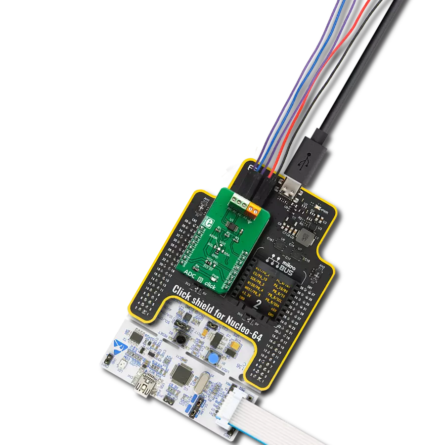
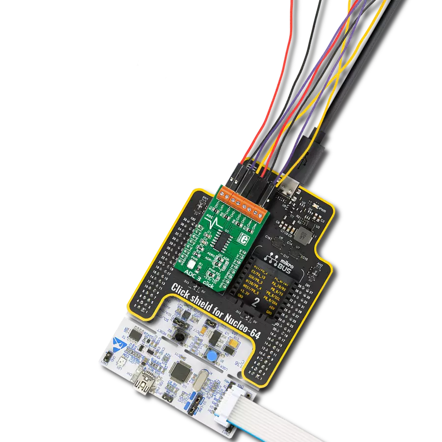
ADC 9 Click
Dev. board
Curiosity Nano with PIC18F57Q43
Compiler
NECTO Studio
MCU
PIC18F57Q43
Experience the power of our ADC and discover what you've been missing
A
A
Hardware Overview
How does it work?
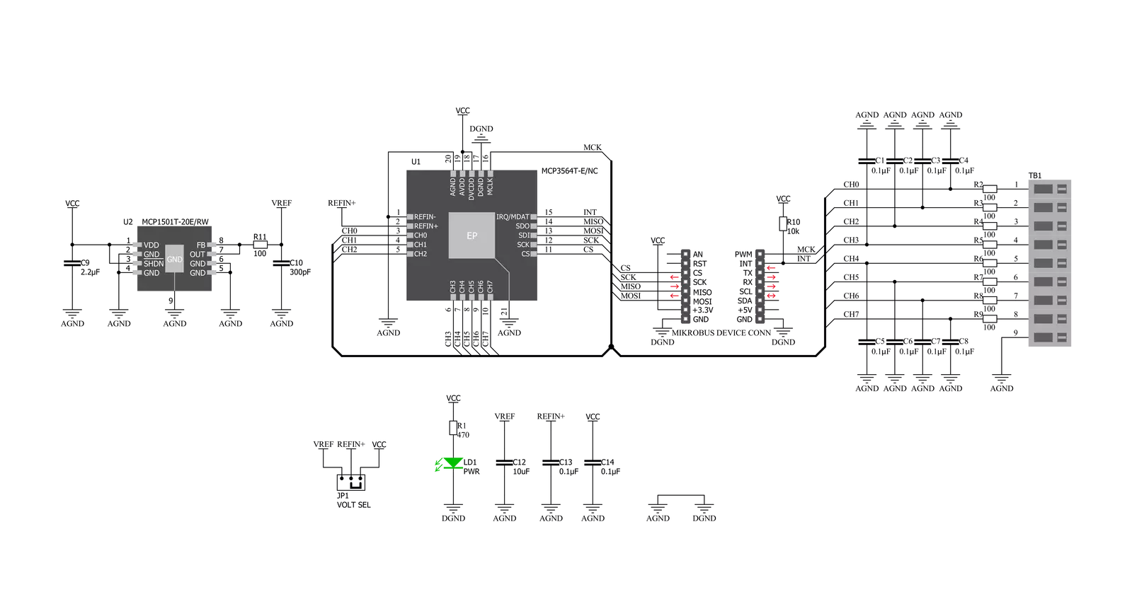
ADC 9 Click is based on MCP3564, a 24-bit Delta-Sigma Analog-to-Digital Converter with a programmable data rate of up to 153.6ksps from Microchip. The MCP3564 is fully configurable with Oversampling Ratio (OSR) from 32 to 98304 and gain from 1/3x to 64x. It includes an internal sequencer (SCAN mode) with multiple monitor channels and a 24-bit timer to automatically create conversion loop sequences without needing MCU communications. Advanced security features, such as CRC and register map lock, can ensure configuration locking and integrity and communication data integrity for secure environments. ADC 9 Click comes with a 20 MHz SPI-compatible serial interface. Communication is simplified with 8-bit commands, including various Continuous Read/Write modes and 24/32-bit multiple data formats that can be accessed by the Direct Memory Access (DMA) of an 8-bit, 16-bit, or 32-bit MCU.
The noise value generally increases when the temperature increases, as thermal noise is dominant for all OSRs larger than 32. For high OSR settings (>512), the thermal noise is dominant and increases proportionally to the square root of the absolute temperature. The noise performance is also a function of the measurement duration. The peak-to-peak noise is usually reduced for short-duration measurements (low number of consecutive samples) because the crest factor (ratio between the RMS noise and peak-to-peak noise) is reduced. This feature is only a consequence of the noise distribution being Gaussian by nature. ADC 9 Click use MCP3564 IC with a fully configurable analog input dual multiplexer that can select which input is connected to each of the two differential input pins (VIN+/VIN-) of the Delta-Sigma ADC. Each of these multiplexers includes the same possibilities for the input selection so that the ADC can convert any
required combination of input voltages. The analog multiplexer comprises parallel low-resistance input switches turned on or off depending on the input channel selection. Their resistance is negligible compared to the input impedance of the ADC (caused by the charge and discharge of the input sampling capacitors on the VIN+/VIN- ADC inputs). ADC 9 Click also features MCP1501, a low drift bandgap-based voltage reference from Microchip for precision data acquisition systems. The bandgap uses chopper-based amplifiers, effectively reducing the drift to zero. This Click board™ can only be operated with a 3.3V logic voltage level. The board must perform appropriate logic voltage level conversion before using MCUs with different logic levels. However, the Click board™ comes equipped with a library containing functions and an example code that can be used as a reference for further development.


Features overview
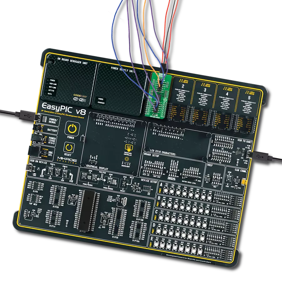
Development board
PIC18F57Q43 Curiosity Nano evaluation kit is a cutting-edge hardware platform designed to evaluate microcontrollers within the PIC18-Q43 family. Central to its design is the inclusion of the powerful PIC18F57Q43 microcontroller (MCU), offering advanced functionalities and robust performance. Key features of this evaluation kit include a yellow user LED and a responsive
mechanical user switch, providing seamless interaction and testing. The provision for a 32.768kHz crystal footprint ensures precision timing capabilities. With an onboard debugger boasting a green power and status LED, programming and debugging become intuitive and efficient. Further enhancing its utility is the Virtual serial port (CDC) and a debug GPIO channel (DGI
GPIO), offering extensive connectivity options. Powered via USB, this kit boasts an adjustable target voltage feature facilitated by the MIC5353 LDO regulator, ensuring stable operation with an output voltage ranging from 1.8V to 5.1V, with a maximum output current of 500mA, subject to ambient temperature and voltage constraints.

Microcontroller Overview
MCU Card / MCU

Architecture
PIC
MCU Memory (KB)
128
Silicon Vendor
Microchip
Pin count
48
RAM (Bytes)
8196
You complete me!
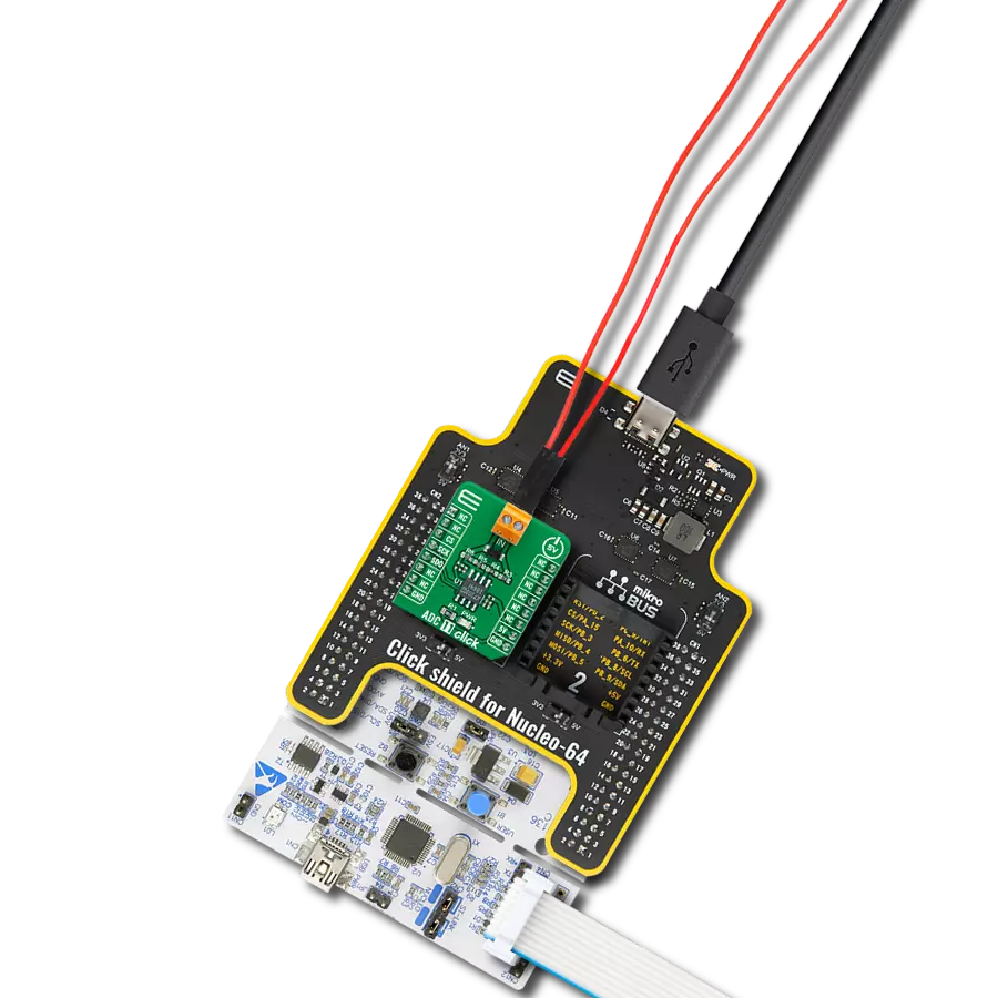
Accessories
Curiosity Nano Base for Click boards is a versatile hardware extension platform created to streamline the integration between Curiosity Nano kits and extension boards, tailored explicitly for the mikroBUS™-standardized Click boards and Xplained Pro extension boards. This innovative base board (shield) offers seamless connectivity and expansion possibilities, simplifying experimentation and development. Key features include USB power compatibility from the Curiosity Nano kit, alongside an alternative external power input option for enhanced flexibility. The onboard Li-Ion/LiPo charger and management circuit ensure smooth operation for battery-powered applications, simplifying usage and management. Moreover, the base incorporates a fixed 3.3V PSU dedicated to target and mikroBUS™ power rails, alongside a fixed 5.0V boost converter catering to 5V power rails of mikroBUS™ sockets, providing stable power delivery for various connected devices.

Used MCU Pins
mikroBUS™ mapper
Take a closer look
Click board™ Schematic
Step by step
Project assembly

Start by selecting your development board and Click board™. Begin with the Curiosity Nano with PIC18F57Q43 as your development board.


Track your results in real time
Application Output
1. Application Output - In Debug mode, the 'Application Output' window enables real-time data monitoring, offering direct insight into execution results. Ensure proper data display by configuring the environment correctly using the provided tutorial.

2. UART Terminal - Use the UART Terminal to monitor data transmission via a USB to UART converter, allowing direct communication between the Click board™ and your development system. Configure the baud rate and other serial settings according to your project's requirements to ensure proper functionality. For step-by-step setup instructions, refer to the provided tutorial.

3. Plot Output - The Plot feature offers a powerful way to visualize real-time sensor data, enabling trend analysis, debugging, and comparison of multiple data points. To set it up correctly, follow the provided tutorial, which includes a step-by-step example of using the Plot feature to display Click board™ readings. To use the Plot feature in your code, use the function: plot(*insert_graph_name*, variable_name);. This is a general format, and it is up to the user to replace 'insert_graph_name' with the actual graph name and 'variable_name' with the parameter to be displayed.

Software Support
Library Description
This library contains API for ADC 9 Click driver.
Key functions:
uint8_t adc9_write_fast_cmd ( uint8_t dev_adr, uint8_t cmd );- Function is used to execute fast command.uint8_t adc9_read_def_adc ( uint8_t dev_adr, int32_t *rd_data );- Function is used to read ADC value when the default fata format is applied.float adc9_volt_calc ( int32_t adc_val, uint16_t v_ref, uint8_t gain );- Function is used to calculate voltage based on ADC values.
Open Source
Code example
The complete application code and a ready-to-use project are available through the NECTO Studio Package Manager for direct installation in the NECTO Studio. The application code can also be found on the MIKROE GitHub account.
/*!
 * \file
 * \brief Adc9 Click example
 *
 * # Description
 * This Click is 8th channel analog to digital converter expansion board, usefull for projects
 * where we have demand for multi channel ADC conversion such as microcontrollers with small
 * number or none analog inputs. It offers integrated features, such as internal oscillator,
 * temperature sensor and burnout sensor detection, in order to reduce system component count
 * and total solution cost.
 *
 * The demo application is composed of two sections :
 *
 * ## Application Init
 * Initalizes SPI driver, resets and starts the device, and makes an initial log.
 *
 * ## Application Task
 * This is an example that shows the capabilities of the ADC 9 Click by calculating voltage level
 * based on ADC from channels 0(positive) and 1(negative), and logs the result.
 *
 * ## Additional Function
 * - void measurement_init ( adc9_t *ctx, adc9_rw_t *rw ) - Measurement Initialization function
 * is used to easily apply desired settings, in this case device is set to read ADC value
 * from channels 0 (positive) and 1 (negative) with default data format, gain, boost and internal clock.
 *
 * ## NOTE
 * Depending on the VOLT SEL jumper position on the Click board the user needs to set VREF
 * macro value (mV) in the code.
 *
 * \author MikroE Team
 *
 */
// ------------------------------------------------------------------- INCLUDES

#include "board.h"
#include "log.h"
#include "adc9.h"

#define VREF  2048

// ------------------------------------------------------------------ VARIABLES

static adc9_t adc9;
static adc9_rw_t adc9_rw;
static log_t logger;

int32_t adc_value;
float m_volts;

// ------------------------------------------------------- ADDITIONAL FUNCTIONS

// Measurement Initialization function
void measurement_init ( adc9_t *ctx, adc9_rw_t *rw )
{
    uint8_t cfg_data;
    uint32_t cfg_data_l;
    uint32_t dummy_data;

    rw->dev_adr = ADC9_DEVICE_ADR;
    rw->reg = ADC9_REG_ADC_DATA;
    rw->cmd = ADC9_CMD_INC_READ;
    adc9_read_u32( ctx, rw, &dummy_data );
    Delay_ms ( 1 );

    rw->reg = ADC9_REG_CFG_0;
    cfg_data = ADC9_CFG_0_VREF_SEL_0 | ADC9_CFG_0_CLK_SEL_2 |
               ADC9_CFG_0_CS_SEL_0 | ADC9_CFG_0_MODE_CONV;
    adc9_write_u8( ctx, rw, cfg_data );
    Delay_ms ( 1 );

    rw->reg = ADC9_REG_CFG_1;
    cfg_data = ADC9_CFG_1_PRE_1 | ADC9_CFG_1_OSR_32 | ADC9_CFG_1_DITHER_DEF;
    adc9_write_u8( ctx, rw, cfg_data );
    Delay_ms ( 1 );

    rw->reg = ADC9_REG_CFG_2;
    cfg_data = ADC9_CFG_2_BOOST_X_1 | ADC9_CFG_2_GAIN_X_1 | ADC9_CFG_2_AZ_MUX_DIS |
               ADC9_CFG_2_AZ_VREF_EN | ADC9_CFG_2_AZ_FREQ_HIGH;
    adc9_write_u8( ctx, rw, cfg_data );
    Delay_ms ( 1 );

    rw->reg = ADC9_REG_CFG_3;
    cfg_data = ADC9_CFG_3_CONV_MODE_CONT | ADC9_CFG_3_DATA_FORMAT_DEF |
               ADC9_CFG_3_CRC_FORMAT_16 | ADC9_CFG_3_CRC_COM_DIS | ADC9_CFG_3_CRC_OFF_CAL_EN |
               ADC9_CFG_3_CRC_GAIN_CAL_EN;
    adc9_write_u8( ctx, rw, cfg_data );
    Delay_ms ( 1 );

    rw->reg = ADC9_REG_MUX;
    cfg_data = ADC9_MUX_VIN_POS_CH0 | ADC9_MUX_VIN_NEG_CH1;
    adc9_write_u8( ctx, rw, cfg_data );
    Delay_ms ( 1 );

    cfg_data_l = 0;
    rw->reg = ADC9_REG_SCAN;
    adc9_write_u24( ctx, rw, cfg_data_l );
    Delay_ms ( 1 );

    cfg_data_l = 0;
    rw->reg = ADC9_REG_OFFSET_CAL;
    adc9_write_u24( ctx, rw, cfg_data_l );
    Delay_ms ( 1 );

    cfg_data_l = 0x00800000;
    rw->reg = ADC9_REG_GAIN_CAL;
    adc9_write_u24( ctx, rw, cfg_data_l );
    Delay_ms ( 1 );

    cfg_data_l = 0x00900F00;
    rw->reg = ADC9_RSV_REG_W_A;
    adc9_write_u24( ctx, rw, cfg_data_l );
    Delay_ms ( 1 );
}

// ------------------------------------------------------ APPLICATION FUNCTIONS

void application_init ( void )
{
    log_cfg_t log_cfg;
    adc9_cfg_t cfg;

    /**
     * Logger initialization.
     * Default baud rate: 115200
     * Default log level: LOG_LEVEL_DEBUG
     * @note If USB_UART_RX and USB_UART_TX
     * are defined as HAL_PIN_NC, you will
     * need to define them manually for log to work.
     * See @b LOG_MAP_USB_UART macro definition for detailed explanation.
     */
    LOG_MAP_USB_UART( log_cfg );
    log_init( &logger, &log_cfg );
    log_info( &logger, "---- Application Init ----" );

    //  Click initialization.

    adc9_cfg_setup( &cfg );
    ADC9_MAP_MIKROBUS( cfg, MIKROBUS_1 );
    uint8_t err_flag = adc9_init( &adc9, &cfg );
    if ( ADC9_INIT_ERROR == err_flag )
    {
        log_info( &logger, "---- Error Init ----" );
        for ( ; ; );
    }

    adc9_default_cfg( &adc9, &adc9_rw );

    Delay_ms ( 1000 );
}

void application_task ( void )
{
    measurement_init( &adc9, &adc9_rw );

    while ( adc9_irq_pin_state( &adc9 ) );

    adc9_rw.reg = ADC9_DEVICE_ADR;
    adc9_read_def_adc ( &adc9, &adc9_rw, &adc_value );

    log_printf( &logger, "ADC Value : %ld\r\n" , adc_value );

    m_volts = adc9_volt_calc ( &adc9, adc_value, VREF, 1 );
    log_printf( &logger, "Voltage in milivolts : %.2f\r\n", m_volts );

    log_printf( &logger, "------------------------\r\n" );
    Delay_ms ( 1000 );
}

int main ( void )
{
    /* Do not remove this line or clock might not be set correctly. */
    #ifdef PREINIT_SUPPORTED
    preinit();
    #endif

    application_init( );

    for ( ; ; )
    {
        application_task( );
    }

    return 0;
}


// ------------------------------------------------------------------------ END
Additional Support
Resources
Category:ADC