Translate digital information into real-world impact with MCP4726 and PIC18F57Q43
Redefine data interpretation

Published Feb 13, 2024
Click board™
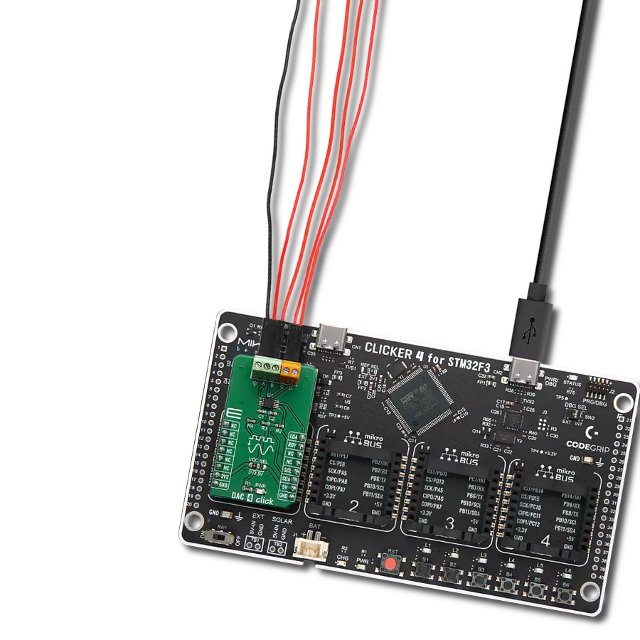
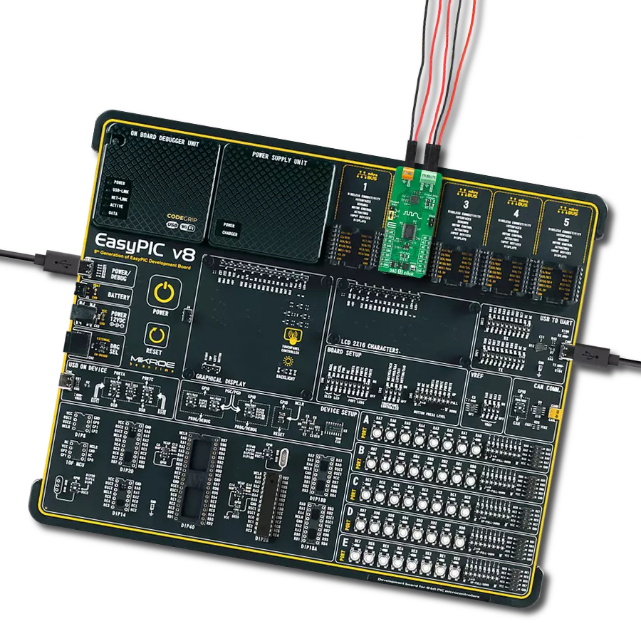
DAC 3 Click
Dev. board
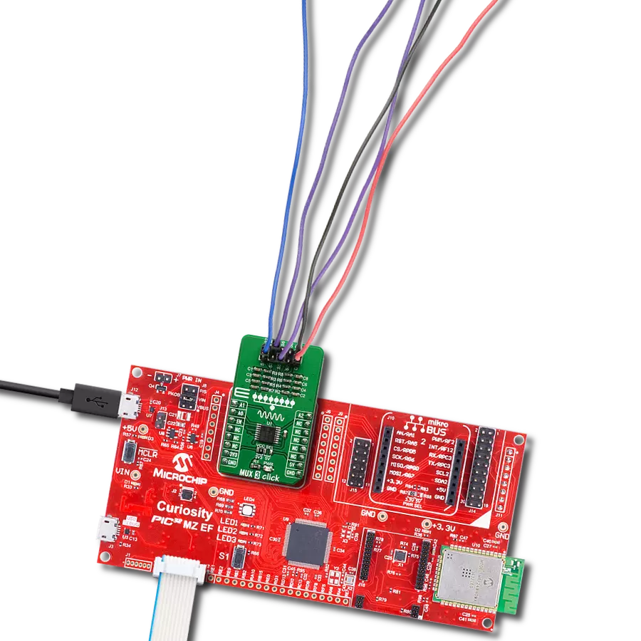
Curiosity Nano with PIC18F57Q43
Compiler
NECTO Studio
MCU
PIC18F57Q43
From binary to brilliance, our DAC technology takes your digital inputs and transforms them into tangible outcomes
A
A
Hardware Overview
How does it work?
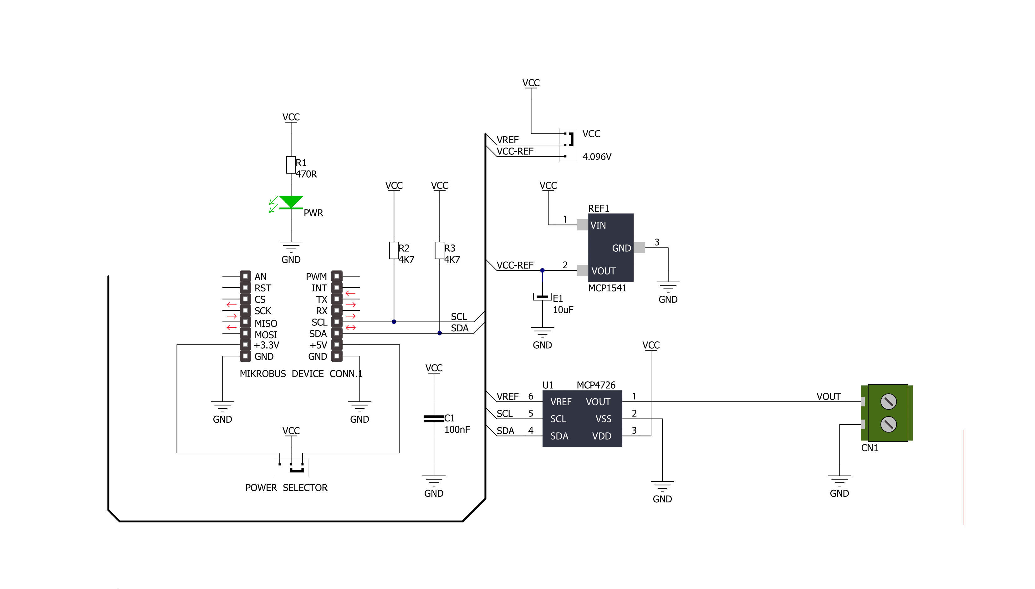
DAC 3 Click is based on the MCP4726, a 12-bit voltage output digital-to-analog converter with EEPROM from Microchip. The MCP4726 uses a resistor ladder architecture with an analog output provided on the VOUT screw terminal. The VOUT can swing from approximately 0V to approximately VCC voltage, in the case of this Click board™, 3.3V and 5V. The resistor ladder DAC is driven from a software-selectable voltage reference source. The reference voltage can be selected between the VCC and the 4.096V given by the MCP1541 via the REF SEL jumper. The VCC
on this jumper is selected by default and depends on the voltage selection over the PWR SEL jumper, with 3.3V set by default. To communicate with the host MCU, the DAC 3 Click uses the I2C interface over the mikroBUS™ socket for standard (100KHz), fast (400KHz), or High-Speed (3.4MHz) mode. The 16-bit data is sent to the DAC through the I2C interface. This interface is also used to store desired Power-on Reset (POR)/Brown-out Reset (BOR) values of the DAC register and device configuration bits. During operation, the internal POR/BOR circuit monitors the power supply
voltage (VCC) and ensures the correct device Start-Up sequence at system power-up and power-down events. This Click board™ can operate with either 3.3V or 5V logic voltage levels selected via the PWR SEL jumper. This way, both 3.3V and 5V capable MCUs can use the communication lines properly. Also, this Click board™ comes equipped with a library containing easy-to-use functions and an example code that can be used as a reference for further development.

Features overview
Development board
PIC18F57Q43 Curiosity Nano evaluation kit is a cutting-edge hardware platform designed to evaluate microcontrollers within the PIC18-Q43 family. Central to its design is the inclusion of the powerful PIC18F57Q43 microcontroller (MCU), offering advanced functionalities and robust performance. Key features of this evaluation kit include a yellow user LED and a responsive
mechanical user switch, providing seamless interaction and testing. The provision for a 32.768kHz crystal footprint ensures precision timing capabilities. With an onboard debugger boasting a green power and status LED, programming and debugging become intuitive and efficient. Further enhancing its utility is the Virtual serial port (CDC) and a debug GPIO channel (DGI
GPIO), offering extensive connectivity options. Powered via USB, this kit boasts an adjustable target voltage feature facilitated by the MIC5353 LDO regulator, ensuring stable operation with an output voltage ranging from 1.8V to 5.1V, with a maximum output current of 500mA, subject to ambient temperature and voltage constraints.

Microcontroller Overview
MCU Card / MCU

Architecture
PIC
MCU Memory (KB)
128
Silicon Vendor
Microchip
Pin count
48
RAM (Bytes)
8196
You complete me!
Accessories
Curiosity Nano Base for Click boards is a versatile hardware extension platform created to streamline the integration between Curiosity Nano kits and extension boards, tailored explicitly for the mikroBUS™-standardized Click boards and Xplained Pro extension boards. This innovative base board (shield) offers seamless connectivity and expansion possibilities, simplifying experimentation and development. Key features include USB power compatibility from the Curiosity Nano kit, alongside an alternative external power input option for enhanced flexibility. The onboard Li-Ion/LiPo charger and management circuit ensure smooth operation for battery-powered applications, simplifying usage and management. Moreover, the base incorporates a fixed 3.3V PSU dedicated to target and mikroBUS™ power rails, alongside a fixed 5.0V boost converter catering to 5V power rails of mikroBUS™ sockets, providing stable power delivery for various connected devices.

Used MCU Pins
mikroBUS™ mapper
Take a closer look
Click board™ Schematic
Step by step
Project assembly

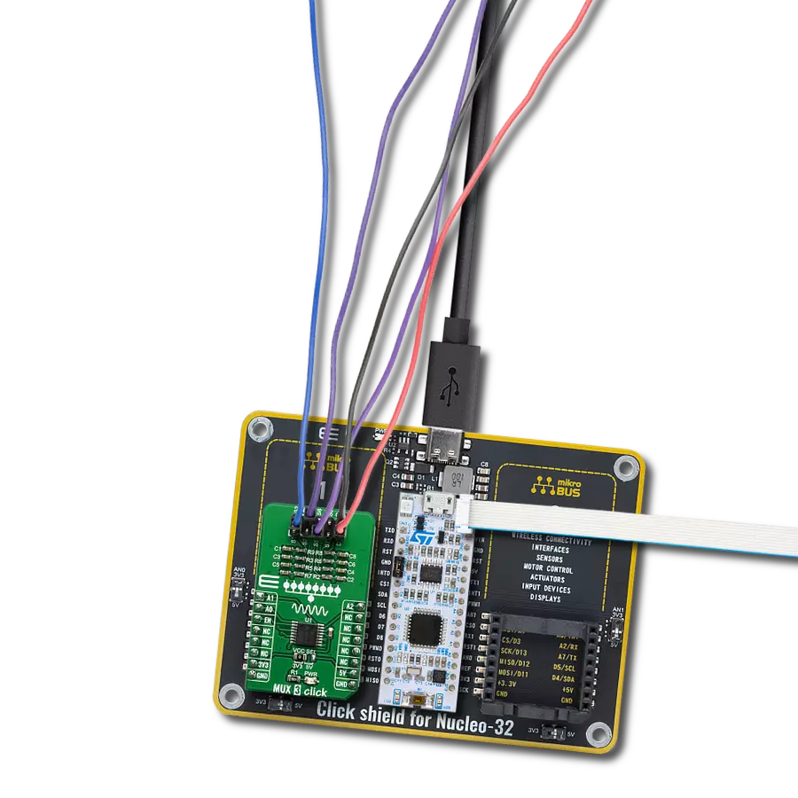
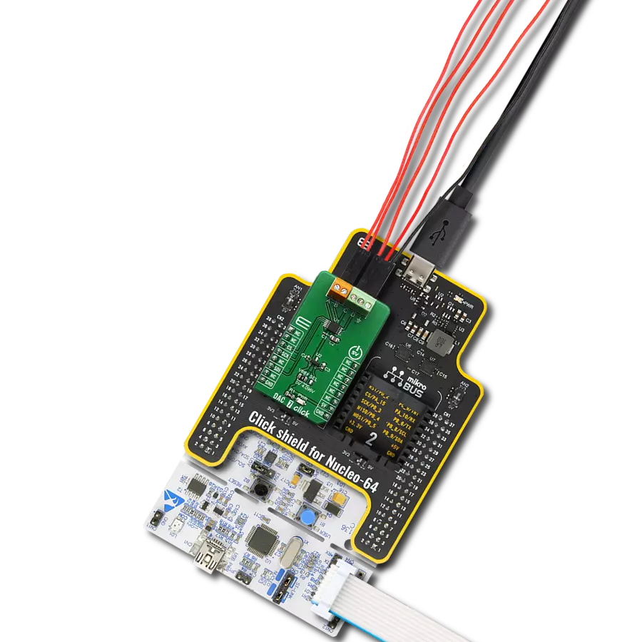
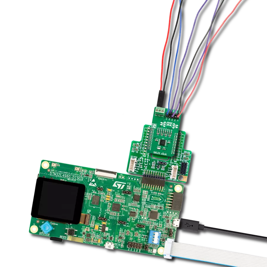
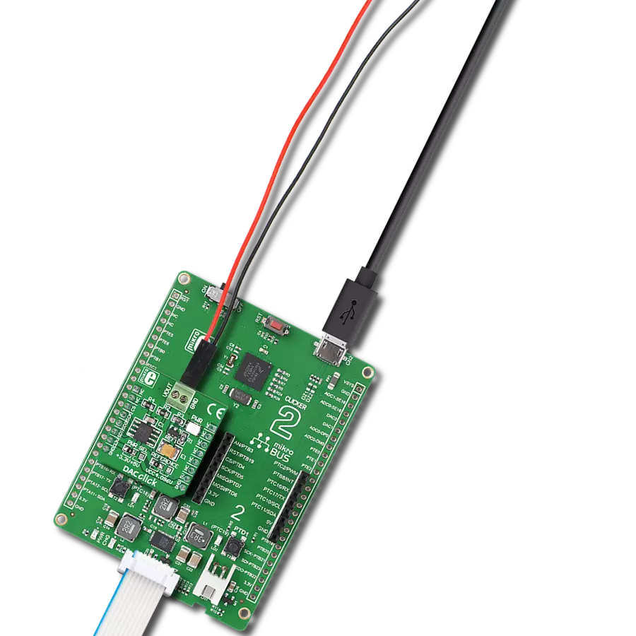
Start by selecting your development board and Click board™. Begin with the Curiosity Nano with PIC18F57Q43 as your development board.


Software Support
Library Description
This library contains API for DAC 3 Click driver.
Key functions:
dac3_write_all_mem- This function configures the click moduledac3_send_command- This function sends a command to the click module using SPI communicationdac3_set_out_voltage- This function sets the output voltage on the click module terminal.
Open Source
Code example
The complete application code and a ready-to-use project are available through the NECTO Studio Package Manager for direct installation in the NECTO Studio. The application code can also be found on the MIKROE GitHub account.
/*!
 * \file
 * \brief DAC3 Click example
 *
 * # Description
 * This example showcases how to initialize, configure and use the DAC 3 Click module. The Click
 * performs digital to analog conversion and the output voltage can be read on the output termi-
 * nal using a multimeter. An oscilloscope is required to read the analog signal.
 *
 * The demo application is composed of two sections :
 *
 * ## Application Init
 * This function configures and initializes the Click and logger modules. The write_all_mem(...)
 * function configures DAC settings.
 *
 * ## Application Task
 * This function resets and wakes up the Click module and then changes the output voltage on the
 * output terminal a few times in a loop with a 5 second delay. It does so every 1 second.
 *
 * \author MikroE Team
 *
 */
// ------------------------------------------------------------------- INCLUDES

#include "board.h"
#include "log.h"
#include "dac3.h"

// ------------------------------------------------------------------ VARIABLES

static dac3_t dac3;
static log_t logger;

// ------------------------------------------------------ APPLICATION FUNCTIONS

void application_init ( )
{
    log_cfg_t log_cfg;
    dac3_cfg_t cfg;

    /**
     * Logger initialization.
     * Default baud rate: 115200
     * Default log level: LOG_LEVEL_DEBUG
     * @note If USB_UART_RX and USB_UART_TX
     * are defined as HAL_PIN_NC, you will
     * need to define them manually for log to work.
     * See @b LOG_MAP_USB_UART macro definition for detailed explanation.
     */
    LOG_MAP_USB_UART( log_cfg );
    log_init( &logger, &log_cfg );
    log_info( &logger, "---- Application Init ----" );

    //  Click initialization.

    dac3_cfg_setup( &cfg );
    DAC3_MAP_MIKROBUS( cfg, MIKROBUS_1 );
    dac3_init( &dac3, &cfg );

    dac3.dac_cfg.vrl = 0;
    dac3.dac_cfg.power = 0;
    dac3.dac_cfg.gain = 0;

    dac3_write_all_mem( &dac3, 0 );
    Delay_100ms( );
}

void application_task ( )
{
    uint8_t cnt;
    uint32_t output_value;

    output_value = 500;

    dac3_send_command( &dac3, DAC3_RESET );
    Delay_100ms( );

    dac3_send_command( &dac3, DAC3_WAKE_UP );
    Delay_100ms( );

    for ( cnt = 1; cnt < 9; cnt ++ )
    {
        dac3_set_out_voltage( &dac3, output_value * cnt );

        log_printf( &logger, " .current DAC value: %d\r\n", output_value * cnt );
        log_printf( &logger, " .output voltage: %d mV\r\n", ( ( output_value * cnt ) * 79 ) / 64 );
        log_printf( &logger, "-------------------------------\r\n" );

        Delay_ms ( 1000 );
        Delay_ms ( 1000 );
        Delay_ms ( 1000 );
        Delay_ms ( 1000 );
        Delay_ms ( 1000 );
    }

    log_printf( &logger, "###############################\r\n" );
    Delay_1sec( );
}

int main ( void )
{
    /* Do not remove this line or clock might not be set correctly. */
    #ifdef PREINIT_SUPPORTED
    preinit();
    #endif

    application_init( );

    for ( ; ; )
    {
        application_task( );
    }

    return 0;
}

// ------------------------------------------------------------------------ END
Additional Support
Resources
Category:DAC