Keep your data protected and secure with AT25FF321A and PIC18F57Q43
A flash that never fades!
Published Feb 13, 2024
Click board™
Flash 10 Click
Dev. board
Curiosity Nano with PIC18F57Q43
Compiler
NECTO Studio
MCU
PIC18F57Q43
Keep data and information stored even when the power is off
A
A
Hardware Overview
How does it work?
Flash 10 Click is based on the AT25FF321A, a highly reliable serial Flash memory solution designed for use in various high-volume consumer and connected applications from Dialog Semiconductor. The AT25FF321A is organized as a 32Mbit (16x2 Mbit physical block) Flash memory ideally suited for systems where program code is shadowed from Flash memory into embedded or external RAM (code shadow) for execution and where small amounts of data are stored and updated locally in the Flash memory. The AT25FF321A specifies a minimum of 100.000 endurance cycles with data retention of a minimum of 20 years, allowing it to handle unlimited reads/writes to the memory. The AT25FF321A's erase block sizes are optimized to meet the needs of today's code and data storage applications, supporting flexible and optimized erase architecture for code and data storage
applications (4kB, 32kB, and 64kB block erase operations) and a full-chip erase feature. Optimizing the erase blocks' size can be the most efficient use of memory space. Also, the AT25FF321A contains four specialized 128-byte One-Time Programmable (OTP) security registers which can be used to store a unique device ID and locked key storage. Flash 10 Click communicates with MCU through a standard SPI interface supporting the two most common SPI modes, SPI Mode 0 and 3. Furthermore, this Click board™ provides additional hardware-controlled functions. The configurable Write Protection, marked as WP and routed on the PWM pin of the mikroBUS™ socket, protects all registers (including status and configuration) from write operations and must be held low to inhibit all the write operations to registers. When this pin is low, all memory and register write
operations are prohibited, and the address counter is not incremented. Also, it is possible to use the Reset or Hold function through the RST pin of the mikroBUS™ socket, depending on the state of the HOLD/RESET bit 7 in Status Register 3. In the case of the Hold function, this pin temporarily pauses serial communication without deselecting or resetting the device, while in the case of the Reset feature, a low logic level on the RST pin puts the AT25FF321A into a Reset state. This Click board™ can only be operated with a 3.3V logic voltage level. The board must perform appropriate logic voltage level conversion before using MCUs with different logic levels. However, the Click board™ comes equipped with a library containing functions and an example code that can be used as a reference for further development.


Features overview
Development board
PIC18F57Q43 Curiosity Nano evaluation kit is a cutting-edge hardware platform designed to evaluate microcontrollers within the PIC18-Q43 family. Central to its design is the inclusion of the powerful PIC18F57Q43 microcontroller (MCU), offering advanced functionalities and robust performance. Key features of this evaluation kit include a yellow user LED and a responsive
mechanical user switch, providing seamless interaction and testing. The provision for a 32.768kHz crystal footprint ensures precision timing capabilities. With an onboard debugger boasting a green power and status LED, programming and debugging become intuitive and efficient. Further enhancing its utility is the Virtual serial port (CDC) and a debug GPIO channel (DGI
GPIO), offering extensive connectivity options. Powered via USB, this kit boasts an adjustable target voltage feature facilitated by the MIC5353 LDO regulator, ensuring stable operation with an output voltage ranging from 1.8V to 5.1V, with a maximum output current of 500mA, subject to ambient temperature and voltage constraints.

Microcontroller Overview
MCU Card / MCU

Architecture
PIC
MCU Memory (KB)
128
Silicon Vendor
Microchip
Pin count
48
RAM (Bytes)
8196
You complete me!
Accessories
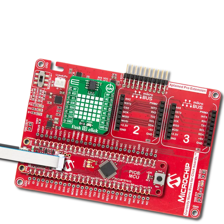
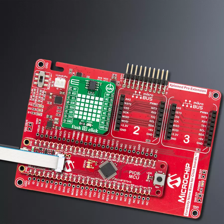
Curiosity Nano Base for Click boards is a versatile hardware extension platform created to streamline the integration between Curiosity Nano kits and extension boards, tailored explicitly for the mikroBUS™-standardized Click boards and Xplained Pro extension boards. This innovative base board (shield) offers seamless connectivity and expansion possibilities, simplifying experimentation and development. Key features include USB power compatibility from the Curiosity Nano kit, alongside an alternative external power input option for enhanced flexibility. The onboard Li-Ion/LiPo charger and management circuit ensure smooth operation for battery-powered applications, simplifying usage and management. Moreover, the base incorporates a fixed 3.3V PSU dedicated to target and mikroBUS™ power rails, alongside a fixed 5.0V boost converter catering to 5V power rails of mikroBUS™ sockets, providing stable power delivery for various connected devices.

Used MCU Pins
mikroBUS™ mapper
Take a closer look
Click board™ Schematic

Step by step
Project assembly

Start by selecting your development board and Click board™. Begin with the Curiosity Nano with PIC18F57Q43 as your development board.


Software Support
Library Description
This library contains API for Flash 10 Click driver.
Key functions:
flash10_erase_memoryThis function erases the selected amount of memory which contains the selected address.flash10_memory_writeThis function writes a desired number of data bytes starting from the selected memory address.flash10_memory_readThis function reads a desired number of data bytes starting from the selected memory address.
Open Source
Code example
The complete application code and a ready-to-use project are available through the NECTO Studio Package Manager for direct installation in the NECTO Studio. The application code can also be found on the MIKROE GitHub account.
/*!
 * @file main.c
 * @brief Flash 10 Click example
 *
 * # Description
 * This example demonstrates the use of Flash 10 Click board by writing specified data to
 * the memory and reading it back.
 *
 * The demo application is composed of two sections :
 *
 * ## Application Init
 * Initializes the driver and checks the communication by reading and verifying the device ID.
 *
 * ## Application Task
 * Writes a desired number of bytes to the memory and then verifies if it is written correctly
 * by reading from the same memory location and displaying the memory content on the USB UART.
 * The whole 4KB block of memory that contains the STARTING_ADDRESS will be erased before writing data.
 *
 * @author Stefan Filipovic
 *
 */

#include "board.h"
#include "log.h"
#include "flash10.h"

#define DEMO_TEXT_MESSAGE_1         "MIKROE"
#define DEMO_TEXT_MESSAGE_2         "Flash 10 Click"
#define STARTING_ADDRESS            0x012345

static flash10_t flash10;
static log_t logger;

void application_init ( void )
{
    log_cfg_t log_cfg;  /**< Logger config object. */
    flash10_cfg_t flash10_cfg;  /**< Click config object. */

    /**
     * Logger initialization.
     * Default baud rate: 115200
     * Default log level: LOG_LEVEL_DEBUG
     * @note If USB_UART_RX and USB_UART_TX
     * are defined as HAL_PIN_NC, you will
     * need to define them manually for log to work.
     * See @b LOG_MAP_USB_UART macro definition for detailed explanation.
     */
    LOG_MAP_USB_UART( log_cfg );
    log_init( &logger, &log_cfg );
    log_info( &logger, " Application Init " );

    // Click initialization.
    flash10_cfg_setup( &flash10_cfg );
    FLASH10_MAP_MIKROBUS( flash10_cfg, MIKROBUS_1 );
    if ( SPI_MASTER_ERROR == flash10_init( &flash10, &flash10_cfg ) )
    {
        log_error( &logger, " Communication init." );
        for ( ; ; );
    }

    if ( FLASH10_ERROR == flash10_check_communication ( &flash10 ) )
    {
        log_error( &logger, " Check communication." );
        for ( ; ; );
    }

    log_info( &logger, " Application Task " );
}

void application_task ( void )
{
    uint8_t data_buf[ 128 ] = { 0 };
    log_printf ( &logger, " Memory address: 0x%.6LX\r\n", ( uint32_t ) STARTING_ADDRESS );
    if ( FLASH10_OK == flash10_erase_memory ( &flash10, FLASH10_CMD_BLOCK_ERASE_4KB, STARTING_ADDRESS ) )
    {
        log_printf ( &logger, " Erase memory block (4KB)\r\n" );
    }
    memcpy ( data_buf, DEMO_TEXT_MESSAGE_1, strlen ( DEMO_TEXT_MESSAGE_1 ) );
    if ( FLASH10_OK == flash10_memory_write ( &flash10, STARTING_ADDRESS,
                                              data_buf, sizeof ( data_buf ) ) )
    {
        log_printf ( &logger, " Write data: %s\r\n", data_buf );
        Delay_ms ( 100 );
    }
    memset ( data_buf, 0, sizeof ( data_buf ) );
    if ( FLASH10_OK == flash10_memory_read ( &flash10, STARTING_ADDRESS,
                                             data_buf, sizeof ( data_buf ) ) )
    {
        log_printf ( &logger, " Read data: %s\r\n\n", data_buf );
        Delay_ms ( 1000 );
        Delay_ms ( 1000 );
        Delay_ms ( 1000 );
    }
    log_printf ( &logger, " Memory address: 0x%.6LX\r\n", ( uint32_t ) STARTING_ADDRESS );
    if ( FLASH10_OK == flash10_erase_memory ( &flash10, FLASH10_CMD_BLOCK_ERASE_4KB, STARTING_ADDRESS ) )
    {
        log_printf ( &logger, " Erase memory block (4KB)\r\n" );
    }
    memcpy ( data_buf, DEMO_TEXT_MESSAGE_2, strlen ( DEMO_TEXT_MESSAGE_2 ) );
    if ( FLASH10_OK == flash10_memory_write ( &flash10, STARTING_ADDRESS,
                                              data_buf, sizeof ( data_buf ) ) )
    {
        log_printf ( &logger, " Write data: %s\r\n", data_buf );
        Delay_ms ( 100 );
    }
    memset ( data_buf, 0, sizeof ( data_buf ) );
    if ( FLASH10_OK == flash10_memory_read ( &flash10, STARTING_ADDRESS,
                                             data_buf, sizeof ( data_buf ) ) )
    {
        log_printf ( &logger, " Read data: %s\r\n\n", data_buf );
        Delay_ms ( 1000 );
        Delay_ms ( 1000 );
        Delay_ms ( 1000 );
    }
}

int main ( void )
{
    /* Do not remove this line or clock might not be set correctly. */
    #ifdef PREINIT_SUPPORTED
    preinit();
    #endif

    application_init( );

    for ( ; ; )
    {
        application_task( );
    }

    return 0;
}

// ------------------------------------------------------------------------ END
Additional Support
Resources
Category:FLASH


