Instantly capture and preserve critical data when power is interrupted thanks to the FM24V10 and PIC18F57Q43
Ferroelectric random-access memory

Published Feb 13, 2024
Click board™
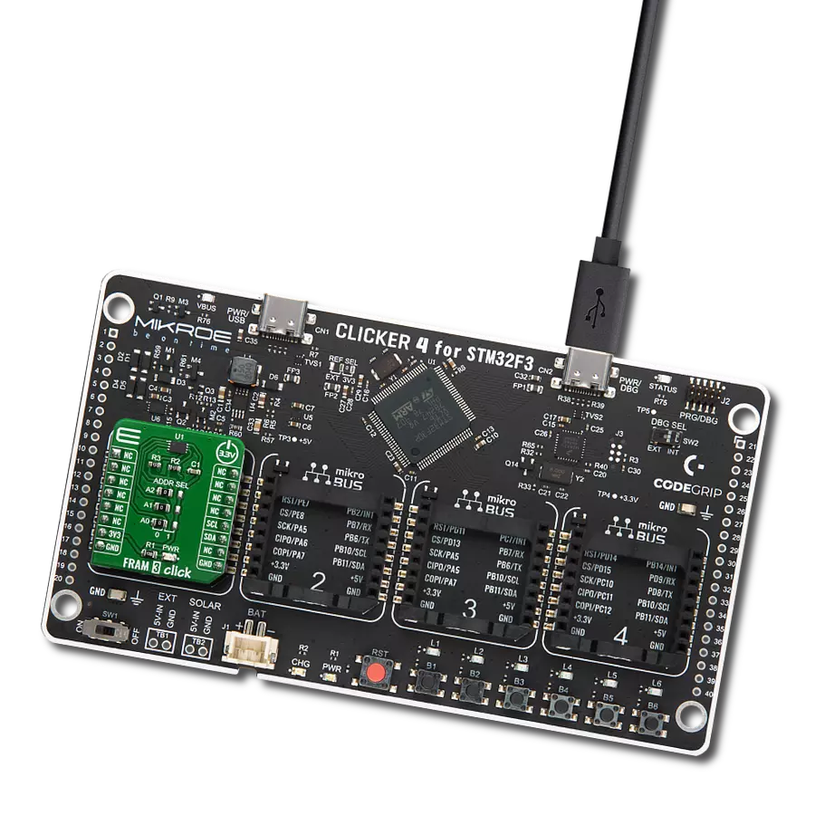
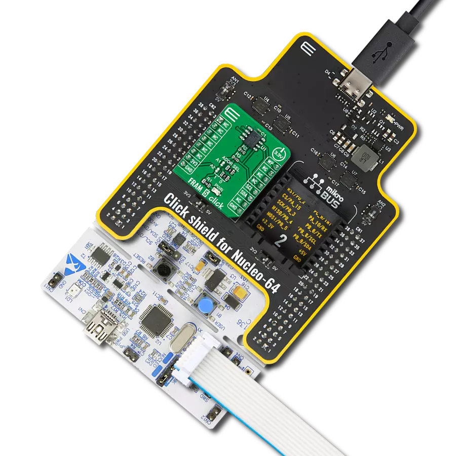
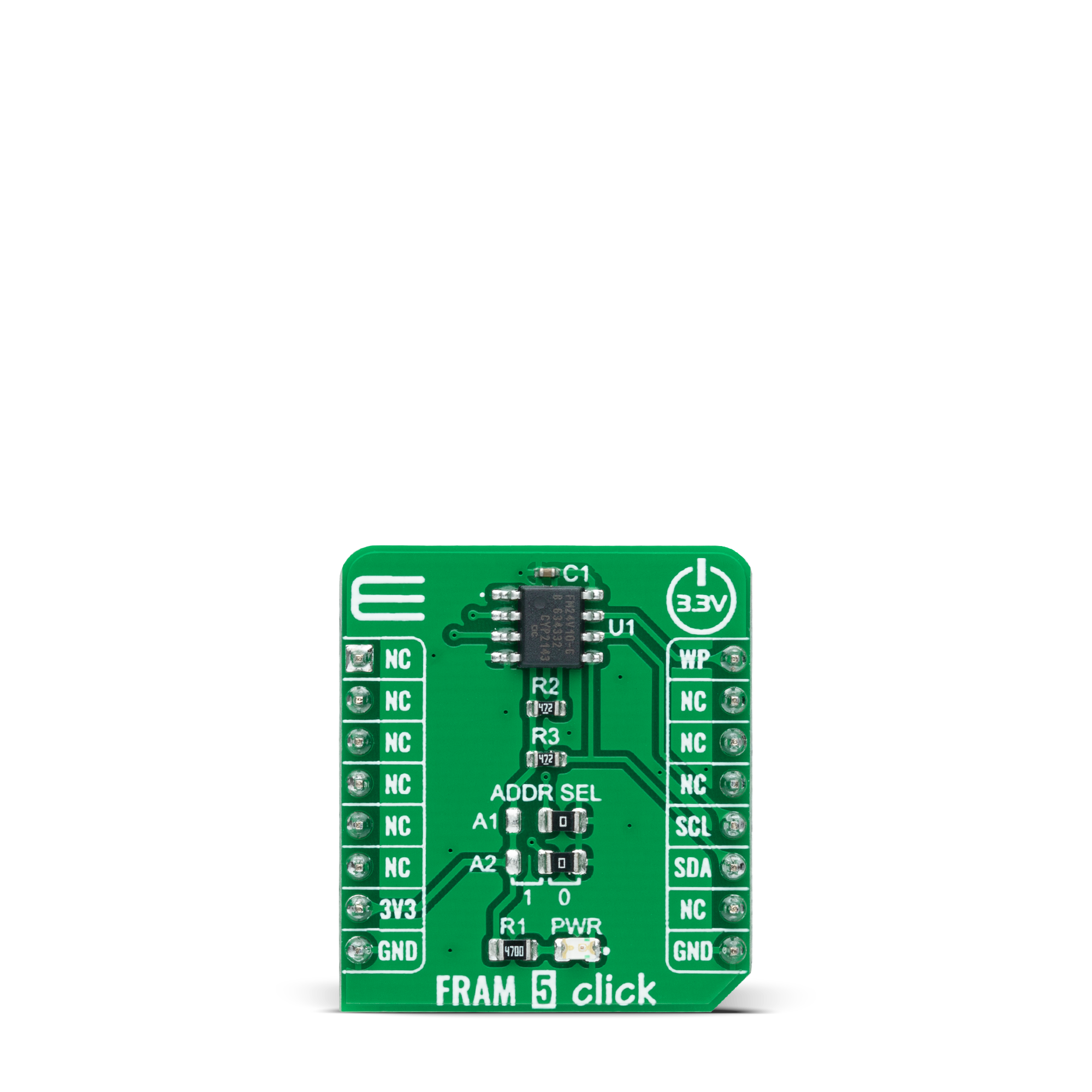
FRAM 5 Click
Dev. board
Curiosity Nano with PIC18F57Q43
Compiler
NECTO Studio
MCU
PIC18F57Q43
Instantly capture and preserve critical data
A
A
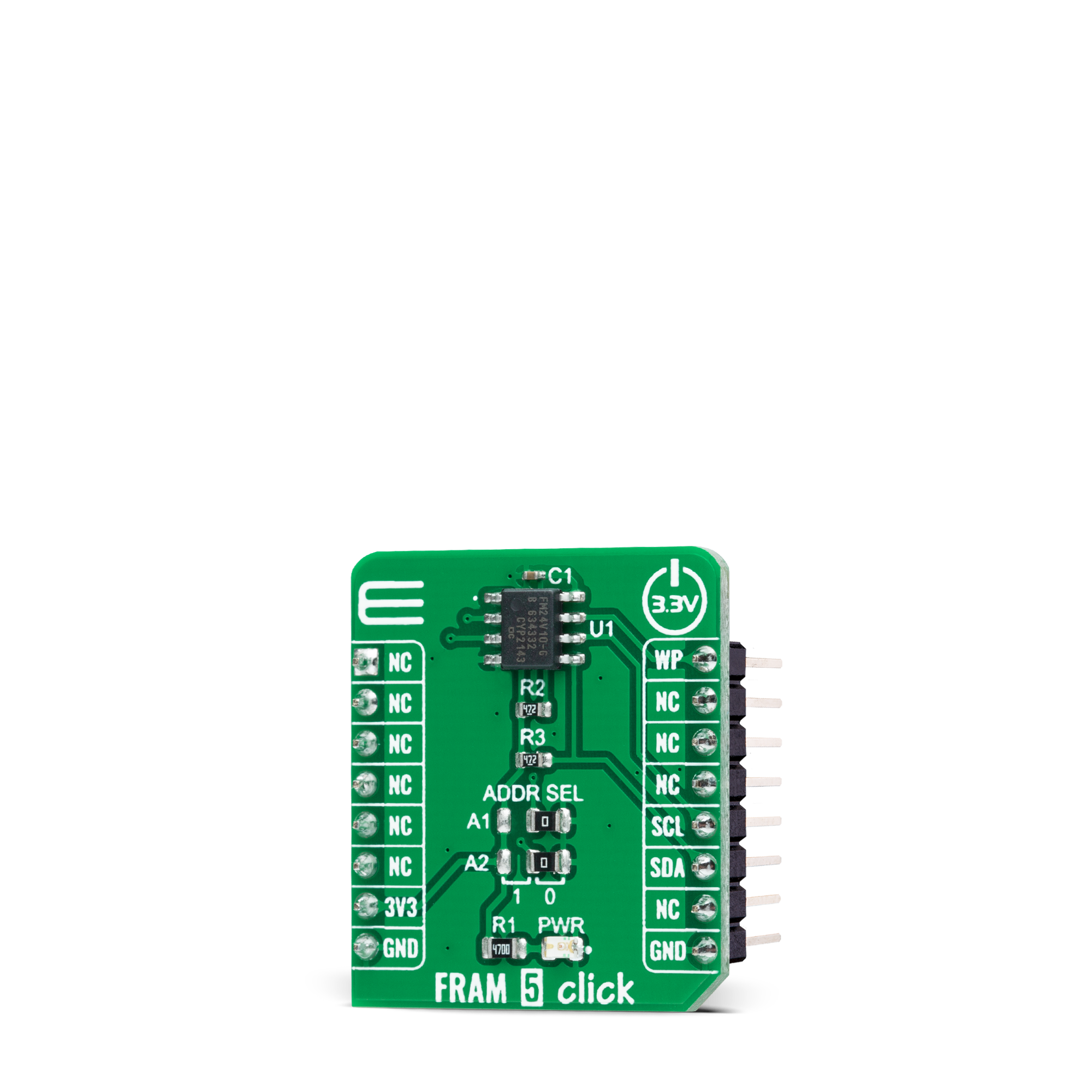
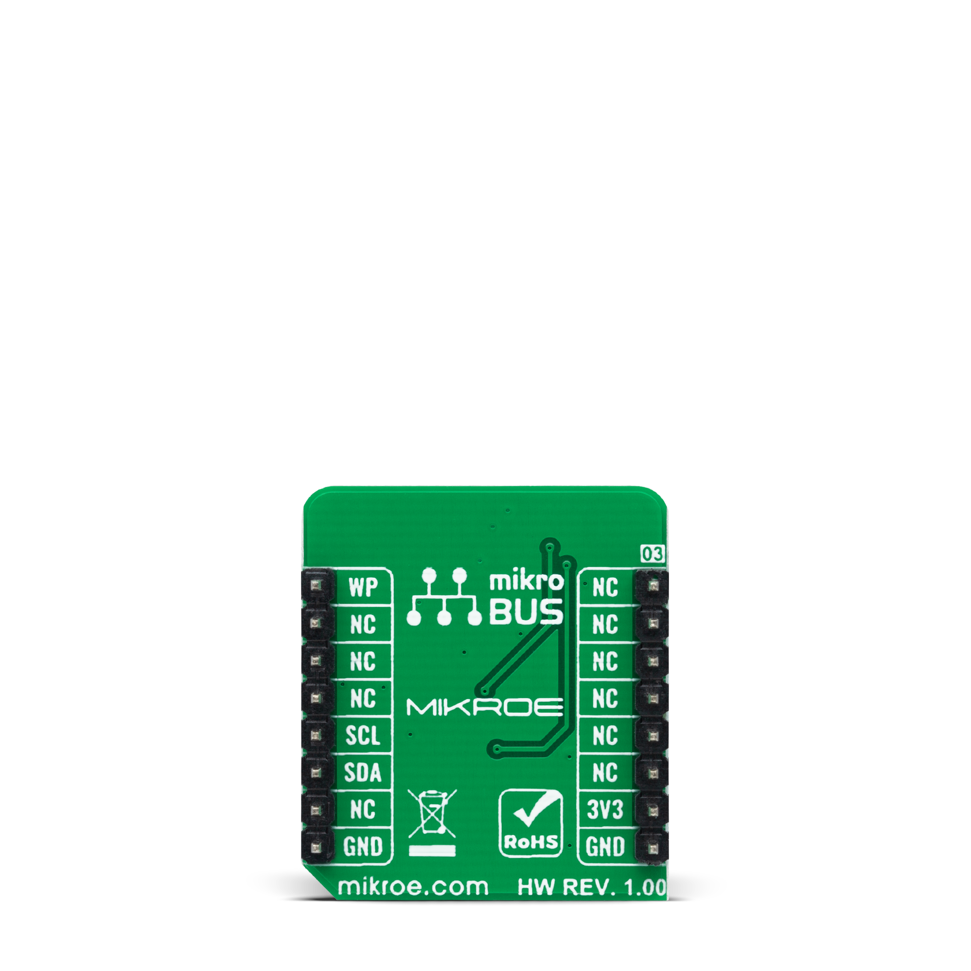
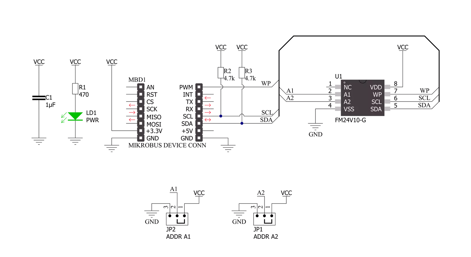
Hardware Overview
How does it work?
FRAM 5 Click is based on the FM24V10, a 1Mbit ferroelectric random access memory (FRAM) logically organized as 131,072×8 bits and accessed using an industry-standard I2C interface from Infineon. The functional operation of the FRAM is similar to serial I2C EEPROM, where the significant difference between the FM24V10 and EEPROM represents the F-RAM's superior write performance, high endurance, and low power consumption. This Click board™ is ideal for nonvolatile memory applications requiring frequent or rapid writes, where example ranges from data collection to demanding industrial controls where the long write time of serial EEPROM can cause data loss. This Click board™ communicates with MCU using the standard
I2C 2-Wire interface, supporting operation with a clock frequency of up to 3.4MHz. Unlike serial EEPROM, the FM24V10 performs write operations at bus speed, where no write delays are incurred. It provides reliable data retention for 151 years while eliminating the complexities, overhead, and system-level reliability problems caused by EEPROM and other nonvolatile memories. It also supports 10 trillion (1014) read/write cycles or 100 million times more write cycles than EEPROM. Besides, the FM24V10 allows choosing its I2C slave address using the SMD jumpers labeled ADDR SEL. The selection can be made by positioning the SMD jumpers to an appropriate position marked as 1 or 0. An additional feature of this FRAM represents
the configurable Write Protection function labeled as WP routed on the PWM pin of the mikroBUS™ socket. The WP pin protects the entire memory and all registers from write operations and must be set to a high logic state to inhibit all the write operations. All memory and register write are prohibited when this pin is high, and the address counter is not incremented. This Click board™ can only be operated with a 3.3V logic voltage level. The board must perform appropriate logic voltage level conversion before using MCUs with different logic levels. However, the Click board™ comes equipped with a library containing functions and an example code that can be used as a reference for further development.
Features overview
Development board
PIC18F57Q43 Curiosity Nano evaluation kit is a cutting-edge hardware platform designed to evaluate microcontrollers within the PIC18-Q43 family. Central to its design is the inclusion of the powerful PIC18F57Q43 microcontroller (MCU), offering advanced functionalities and robust performance. Key features of this evaluation kit include a yellow user LED and a responsive
mechanical user switch, providing seamless interaction and testing. The provision for a 32.768kHz crystal footprint ensures precision timing capabilities. With an onboard debugger boasting a green power and status LED, programming and debugging become intuitive and efficient. Further enhancing its utility is the Virtual serial port (CDC) and a debug GPIO channel (DGI
GPIO), offering extensive connectivity options. Powered via USB, this kit boasts an adjustable target voltage feature facilitated by the MIC5353 LDO regulator, ensuring stable operation with an output voltage ranging from 1.8V to 5.1V, with a maximum output current of 500mA, subject to ambient temperature and voltage constraints.

Microcontroller Overview
MCU Card / MCU

Architecture
PIC
MCU Memory (KB)
128
Silicon Vendor
Microchip
Pin count
48
RAM (Bytes)
8196
You complete me!
Accessories
Curiosity Nano Base for Click boards is a versatile hardware extension platform created to streamline the integration between Curiosity Nano kits and extension boards, tailored explicitly for the mikroBUS™-standardized Click boards and Xplained Pro extension boards. This innovative base board (shield) offers seamless connectivity and expansion possibilities, simplifying experimentation and development. Key features include USB power compatibility from the Curiosity Nano kit, alongside an alternative external power input option for enhanced flexibility. The onboard Li-Ion/LiPo charger and management circuit ensure smooth operation for battery-powered applications, simplifying usage and management. Moreover, the base incorporates a fixed 3.3V PSU dedicated to target and mikroBUS™ power rails, alongside a fixed 5.0V boost converter catering to 5V power rails of mikroBUS™ sockets, providing stable power delivery for various connected devices.

Used MCU Pins
mikroBUS™ mapper
Take a closer look
Click board™ Schematic
Step by step
Project assembly

Start by selecting your development board and Click board™. Begin with the Curiosity Nano with PIC18F57Q43 as your development board.


Track your results in real time
Application Output
1. Application Output - In Debug mode, the 'Application Output' window enables real-time data monitoring, offering direct insight into execution results. Ensure proper data display by configuring the environment correctly using the provided tutorial.

2. UART Terminal - Use the UART Terminal to monitor data transmission via a USB to UART converter, allowing direct communication between the Click board™ and your development system. Configure the baud rate and other serial settings according to your project's requirements to ensure proper functionality. For step-by-step setup instructions, refer to the provided tutorial.

3. Plot Output - The Plot feature offers a powerful way to visualize real-time sensor data, enabling trend analysis, debugging, and comparison of multiple data points. To set it up correctly, follow the provided tutorial, which includes a step-by-step example of using the Plot feature to display Click board™ readings. To use the Plot feature in your code, use the function: plot(*insert_graph_name*, variable_name);. This is a general format, and it is up to the user to replace 'insert_graph_name' with the actual graph name and 'variable_name' with the parameter to be displayed.

Software Support
Library Description
This library contains API for FRAM 5 Click driver.
Key functions:
fram5_check_communicationThis function checks the communication by reading and verifying the device ID.fram5_memory_writeThis function writes a desired number of data bytes starting from the selected memory address.fram5_memory_readThis function reads a desired number of data bytes starting from the selected memory address.
Open Source
Code example
The complete application code and a ready-to-use project are available through the NECTO Studio Package Manager for direct installation in the NECTO Studio. The application code can also be found on the MIKROE GitHub account.
/*!
 * @file main.c
 * @brief FRAM5 Click example
 *
 * # Description
 * This example demonstrates the use of FRAM 5 Click board by writing specified data to
 * the memory and reading it back.
 *
 * The demo application is composed of two sections :
 *
 * ## Application Init
 * Initializes the driver and checks the communication with the Click board.
 *
 * ## Application Task
 * Writes a desired number of bytes to the memory and then verifies that it's written correctly
 * by reading from the same memory location and displaying the memory content on the USB UART.
 *
 * @author Stefan Filipovic
 *
 */

#include "board.h"
#include "log.h"
#include "fram5.h"

static fram5_t fram5;
static log_t logger;

#define DEMO_TEXT_MESSAGE           "MikroE - FRAM 5 Click board"
#define STARTING_ADDRESS            0x01234

void application_init ( void )
{
    log_cfg_t log_cfg;  /**< Logger config object. */
    fram5_cfg_t fram5_cfg;  /**< Click config object. */

    /**
     * Logger initialization.
     * Default baud rate: 115200
     * Default log level: LOG_LEVEL_DEBUG
     * @note If USB_UART_RX and USB_UART_TX
     * are defined as HAL_PIN_NC, you will
     * need to define them manually for log to work.
     * See @b LOG_MAP_USB_UART macro definition for detailed explanation.
     */
    LOG_MAP_USB_UART( log_cfg );
    log_init( &logger, &log_cfg );
    log_info( &logger, " Application Init " );

    // Click initialization.
    fram5_cfg_setup( &fram5_cfg );
    FRAM5_MAP_MIKROBUS( fram5_cfg, MIKROBUS_1 );
    if ( I2C_MASTER_ERROR == fram5_init( &fram5, &fram5_cfg ) )
    {
        log_error( &logger, " Communication init." );
        for ( ; ; );
    }

    if ( FRAM5_ERROR == fram5_check_communication ( &fram5 ) )
    {
        log_error( &logger, " Check communication." );
        for ( ; ; );
    }

    log_info( &logger, " Application Task " );
}

void application_task ( void )
{
    uint8_t data_buf[ 128 ] = { 0 };
    if ( FRAM5_OK == fram5_memory_write ( &fram5, STARTING_ADDRESS,
                                          DEMO_TEXT_MESSAGE, strlen ( DEMO_TEXT_MESSAGE ) ) )
    {
        log_printf ( &logger, "Data written to address 0x%.5lx: %s\r\n", ( uint32_t ) STARTING_ADDRESS,
                                                                           ( char * ) DEMO_TEXT_MESSAGE );
    }
    if ( FRAM5_OK == fram5_memory_read ( &fram5, STARTING_ADDRESS,
                                         data_buf, strlen ( DEMO_TEXT_MESSAGE ) ) )
    {
        log_printf ( &logger, "Data read from address  0x%.5lx: %s\r\n\n", ( uint32_t ) STARTING_ADDRESS,
                                                                                        data_buf );
        Delay_ms ( 1000 );
        Delay_ms ( 1000 );
        Delay_ms ( 1000 );
    }
}

int main ( void )
{
    /* Do not remove this line or clock might not be set correctly. */
    #ifdef PREINIT_SUPPORTED
    preinit();
    #endif

    application_init( );

    for ( ; ; )
    {
        application_task( );
    }

    return 0;
}

// ------------------------------------------------------------------------ END
Additional Support
Resources
Category:FRAM