Enhance access control and security measures with PN5180A0HN and PIC18F57Q43
Your world, just a touch away: Embrace the NFC experience
Published Feb 13, 2024
Click board™
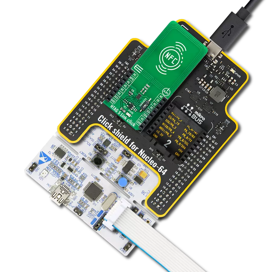
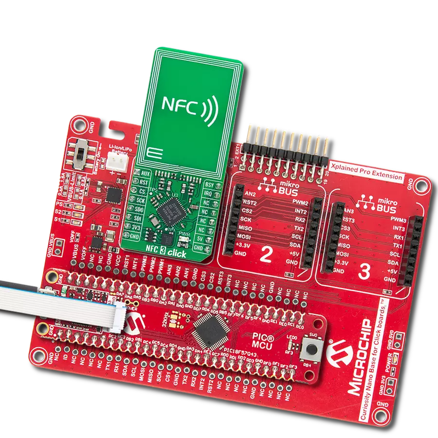
NFC 3 Click
Dev. board
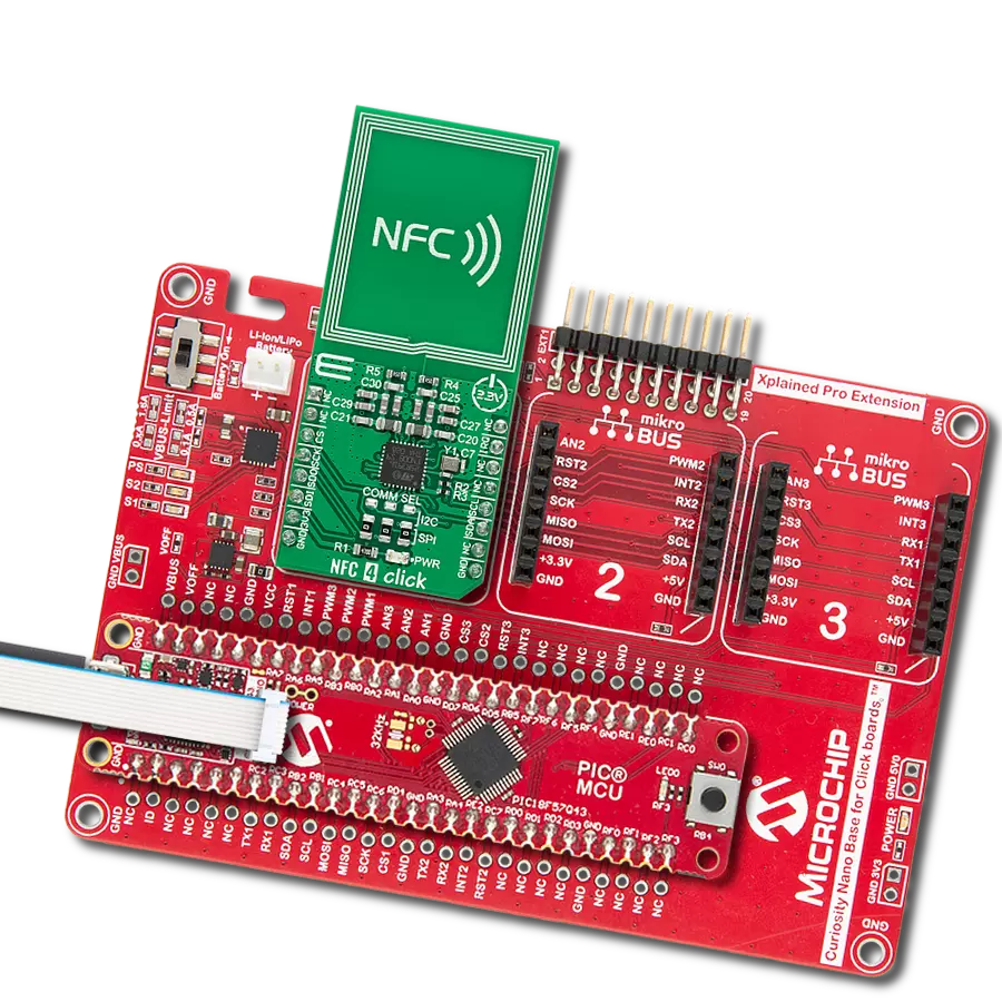
Curiosity Nano with PIC18F57Q43
Compiler
NECTO Studio
MCU
PIC18F57Q43
Step into a future where NFC simplifies and enhances your daily life, offering the convenience of secure payments and instant data sharing
A
A
Hardware Overview
How does it work?
NFC 3 Click is based on the PN5180A0HN, a high-performance multiprotocol full NFC frontend from NXP Semiconductors, for contactless communication at 13.56MHz. The PN5180A0HN implements the RF and all the low-level functionality, like an antenna driving and receiver circuitry, to realize an NFC Forum-compliant reader. It utilizes an outstanding modulation and demodulation concept for different contactless communication methods and protocols. The PN5180A0HN is fully compliant with many Reader/Writer standards like ISO 14443A/B up to 848 kBit/s, JIS X 6319-4 comparable with FeliCa scheme, ISO 15693, ISO 18092, and more. Alongside support for reading all NFC tag types (type 1, 2, 3, 4A, and 4B) and high RF output power, this Click board™ is ideally suited for industrial and consumer NFC applications like industrial, eGov readers, payment terminals, and more. This Click board™ connects to a host MCU with an SPI
interface for configuration, NFC data exchange, and high-level NFC protocol implementation. It supports the most common SPI Mode 0 and operates with data rates up to 7 Mbit/s. The PN5180A0HN has two types of integrated memories: RAM and EEPROM. Internal registers of the PN5180A0HN store configuration data, while the RF configuration for dedicated RF protocols is defined by EEPROM data, copied by a command issued from the host MCU. This allows users to achieve maximum RF performance from a given antenna design. In addition to the SPI interface signals, this board uses several other signals from the mikroBUS™ socket. The reset pin routed on the RST pin of the mikroBUS™ socket provides the general reset ability, while the IRQ pin of the mikroBUS™ socket represents an interrupt request to inform the host controller of various events. The PN5180A0HN also has the possibility of updating the implemented firmware. In Secure
Firmware update mode, the PN5180A0HN requires dedicated physical handling of the SPI interface lines and the BSY line of the mikroBUS™ socket. The BSY signal is used to indicate that the PN5180A0HN is not able to send or receive data over the SPI interface. The secure firmware download mode is entered by setting the AUX pin to a high logic state during the Start-Up sequence of the device. The AUX pin is allowed for any other functionality after Start-Up (as test signals provided by test points on the board); the level of this pin has no impact on the download functionality after Start-Up during standard NFC operation. This Click board™ can be operated only with a 3.3V logic voltage level. The board must perform appropriate logic voltage level conversion before using MCUs with different logic levels. Also, it comes equipped with a library containing functions and an example code that can be used as a reference for further development.


Features overview
Development board
PIC18F57Q43 Curiosity Nano evaluation kit is a cutting-edge hardware platform designed to evaluate microcontrollers within the PIC18-Q43 family. Central to its design is the inclusion of the powerful PIC18F57Q43 microcontroller (MCU), offering advanced functionalities and robust performance. Key features of this evaluation kit include a yellow user LED and a responsive
mechanical user switch, providing seamless interaction and testing. The provision for a 32.768kHz crystal footprint ensures precision timing capabilities. With an onboard debugger boasting a green power and status LED, programming and debugging become intuitive and efficient. Further enhancing its utility is the Virtual serial port (CDC) and a debug GPIO channel (DGI
GPIO), offering extensive connectivity options. Powered via USB, this kit boasts an adjustable target voltage feature facilitated by the MIC5353 LDO regulator, ensuring stable operation with an output voltage ranging from 1.8V to 5.1V, with a maximum output current of 500mA, subject to ambient temperature and voltage constraints.

Microcontroller Overview
MCU Card / MCU

Architecture
PIC
MCU Memory (KB)
128
Silicon Vendor
Microchip
Pin count
48
RAM (Bytes)
8196
You complete me!
Accessories
Curiosity Nano Base for Click boards is a versatile hardware extension platform created to streamline the integration between Curiosity Nano kits and extension boards, tailored explicitly for the mikroBUS™-standardized Click boards and Xplained Pro extension boards. This innovative base board (shield) offers seamless connectivity and expansion possibilities, simplifying experimentation and development. Key features include USB power compatibility from the Curiosity Nano kit, alongside an alternative external power input option for enhanced flexibility. The onboard Li-Ion/LiPo charger and management circuit ensure smooth operation for battery-powered applications, simplifying usage and management. Moreover, the base incorporates a fixed 3.3V PSU dedicated to target and mikroBUS™ power rails, alongside a fixed 5.0V boost converter catering to 5V power rails of mikroBUS™ sockets, providing stable power delivery for various connected devices.

Used MCU Pins
mikroBUS™ mapper
Take a closer look
Click board™ Schematic

Step by step
Project assembly

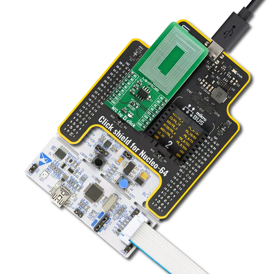
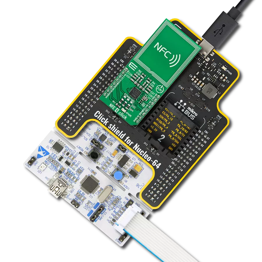
Start by selecting your development board and Click board™. Begin with the Curiosity Nano with PIC18F57Q43 as your development board.


Track your results in real time
Application Output
1. Application Output - In Debug mode, the 'Application Output' window enables real-time data monitoring, offering direct insight into execution results. Ensure proper data display by configuring the environment correctly using the provided tutorial.

2. UART Terminal - Use the UART Terminal to monitor data transmission via a USB to UART converter, allowing direct communication between the Click board™ and your development system. Configure the baud rate and other serial settings according to your project's requirements to ensure proper functionality. For step-by-step setup instructions, refer to the provided tutorial.

3. Plot Output - The Plot feature offers a powerful way to visualize real-time sensor data, enabling trend analysis, debugging, and comparison of multiple data points. To set it up correctly, follow the provided tutorial, which includes a step-by-step example of using the Plot feature to display Click board™ readings. To use the Plot feature in your code, use the function: plot(*insert_graph_name*, variable_name);. This is a general format, and it is up to the user to replace 'insert_graph_name' with the actual graph name and 'variable_name' with the parameter to be displayed.

Software Support
Library Description
This library contains API for NFC 3 Click driver.
Key functions:
nfc3_read_card_uid- NFC 3 read card UID function.nfc3_read_firmware_version- NFC 3 reading firmware version function.nfc3_read_eeprom_version- NFC 3 reading EEPROM version function.
Open Source
Code example
The complete application code and a ready-to-use project are available through the NECTO Studio Package Manager for direct installation in the NECTO Studio. The application code can also be found on the MIKROE GitHub account.
/*!
 * @file main.c
 * @brief NFC3 Click example
 *
 * # Description
 * This example demonstrates the use of NFC 3 Click board
 * by reading MIFARE ISO/IEC 14443 type A tag UID.
 *
 * The demo application is composed of two sections :
 *
 * ## Application Init
 * Initializes driver and logger, then enables the Click board and reads
 * the device product, firmware and eeprom versions.
 *
 * ## Application Task
 * If there's a tag detected, it reads its UID and displays it on USB UART.
 *
 * @note
 * Only tags with 4-byte or 7-byte UIDs are compatible with this example.
 * We recommend MIKROE-1475 - an RFiD tag 13.56MHz compliant with ISO14443-A standard.
 *
 * @author Stefan Filipovic
 *
 */

#include "board.h"
#include "log.h"
#include "nfc3.h"

static nfc3_t nfc3;
static log_t logger;
static uint16_t info;

void application_init ( void )
{
    log_cfg_t log_cfg;  /**< Logger config object. */
    nfc3_cfg_t nfc3_cfg;  /**< Click config object. */

    /**
     * Logger initialization.
     * Default baud rate: 115200
     * Default log level: LOG_LEVEL_DEBUG
     * @note If USB_UART_RX and USB_UART_TX
     * are defined as HAL_PIN_NC, you will
     * need to define them manually for log to work.
     * See @b LOG_MAP_USB_UART macro definition for detailed explanation.
     */
    LOG_MAP_USB_UART( log_cfg );
    log_init( &logger, &log_cfg );
    log_info( &logger, " Application Init " );

    // Click initialization.

    nfc3_cfg_setup( &nfc3_cfg );
    NFC3_MAP_MIKROBUS( nfc3_cfg, MIKROBUS_1 );
    err_t init_flag = nfc3_init( &nfc3, &nfc3_cfg );
    if ( init_flag == SPI_MASTER_ERROR )
    {
        log_error( &logger, " Application Init Error. " );
        log_info( &logger, " Please, run program again... " );
        for ( ; ; );
    }

    nfc3_reset ( &nfc3 );
    Delay_ms ( 100 );

    log_printf( &logger, "------------------------\r\n" );
    nfc3_read_product_version ( &nfc3, &info );
    log_printf( &logger, "Product version: 0x%.4X\r\n", info );
    nfc3_read_firmware_version ( &nfc3, &info );
    log_printf( &logger, "Firmware version: 0x%.4X\r\n", info );
    nfc3_read_eeprom_version ( &nfc3, &info );
    log_printf( &logger, "EEPROM version: 0x%.4X\r\n", info );
    log_printf( &logger, "------------------------\r\n" );
    log_info( &logger, " Application Task " );
    log_printf( &logger, "------------------------\r\n" );
    Delay_ms ( 1000 );
}

void application_task ( void )
{
    uint8_t uid[ 7 ];
    uint8_t uid_len;
    uid_len = nfc3_read_card_uid( &nfc3, uid );
    if ( uid_len > 0 )
    {
        log_printf( &logger, "Tag UID: " );
        for ( uint8_t cnt = 0; cnt < uid_len; cnt++ )
        {
            log_printf( &logger, "0x%.2X ", ( uint16_t ) uid[ cnt ] );
        }
        log_printf( &logger, "\r\n------------------------\r\n" );
        Delay_ms ( 1000 );
    }
}

int main ( void )
{
    /* Do not remove this line or clock might not be set correctly. */
    #ifdef PREINIT_SUPPORTED
    preinit();
    #endif

    application_init( );

    for ( ; ; )
    {
        application_task( );
    }

    return 0;
}

// ------------------------------------------------------------------------ END
Additional Support
Resources
Category:RFID/NFC