Achieve rapid conversion of analog signals into digital form with AD7490 and ATmega328P
12-bit high speed, low power, 16-channel, successive approximation ADC

Published Mar 21, 2024
Click board™
ADC 24 Click
Dev. board
Arduino UNO Rev3
Compiler
NECTO Studio
MCU
ATmega328P
Invaluable tool for developers needing precise monitoring and data analysis solutions
A
A
Hardware Overview
How does it work?
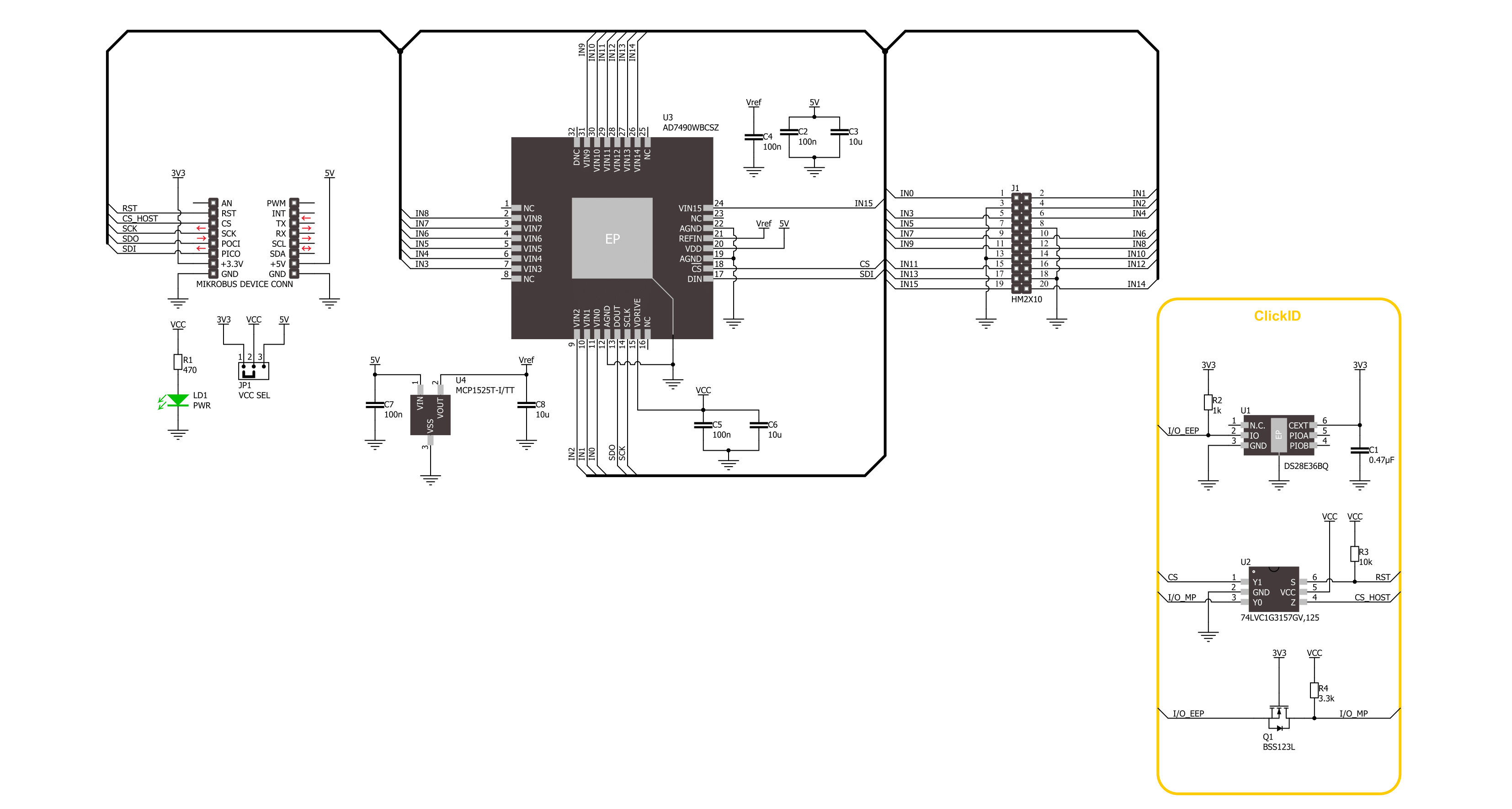
ADC 24 Click is based on the AD7490, a 12-bit, high-speed, low-power, 16-channel successive approximation ADC from Analog Devices. This ADC minimizes power consumption while maintaining high throughput rates, drawing just 2.5mA from a 5V supply at full capacity. It achieves up to 1MSPS throughput rates and incorporates a low noise, wide bandwidth track-and-hold amplifier that adeptly handles input frequencies beyond 1MHz. This Click board™ is particularly suited for applications requiring extensive system monitoring, such as multichannel system monitoring, power line monitoring, data acquisition, instrumentation, and process control. The AD7490 is equipped with 16 single-ended analog inputs, enhanced by a channel sequencer that enables the programmed and
sequential conversion of channels. The analog input range is configurable, offering a 0V to REFIN or a broader 0V to 2×REFIN range, achieved by the MCP1525 voltage reference from Microchip, with fixed 2.5V output. This flexibility allows users to tailor the ADC to various measurement requirements. For accurate utilization of the 0V to 2×REFIN measurement range, powering the IC with 5V is mandatory, which is achieved with 5V from the mikroBUS™ power rail. Moreover, the AD7490 supports multiple operational modes, such as Normal, Full Shutdown, Auto Shutdown, and Auto Standby, all of which are register-configurable. These modes provide users with various power management options to optimize the balance between power dissipation and throughput rate
based on specific application needs. The conversion process and data acquisition are made using CS and the serial clock signal, ensuring straightforward interfacing with microprocessors or DSPs (SPI/QSPI™/MICROWIRE™/ DSP compatible). The input signal is sampled at the falling edge of CS, initiating conversion at this juncture without any pipeline delays. This Click board™ can operate with either 3.3V or 5V logic voltage levels selected via the VCC SEL jumper. This way, both 3.3V and 5V capable MCUs can use the communication lines properly. Also, this Click board™ comes equipped with a library containing easy-to-use functions and an example code that can be used as a reference for further development.

Features overview
Development board
Arduino UNO is a versatile microcontroller board built around the ATmega328P chip. It offers extensive connectivity options for various projects, featuring 14 digital input/output pins, six of which are PWM-capable, along with six analog inputs. Its core components include a 16MHz ceramic resonator, a USB connection, a power jack, an
ICSP header, and a reset button, providing everything necessary to power and program the board. The Uno is ready to go, whether connected to a computer via USB or powered by an AC-to-DC adapter or battery. As the first USB Arduino board, it serves as the benchmark for the Arduino platform, with "Uno" symbolizing its status as the
first in a series. This name choice, meaning "one" in Italian, commemorates the launch of Arduino Software (IDE) 1.0. Initially introduced alongside version 1.0 of the Arduino Software (IDE), the Uno has since become the foundational model for subsequent Arduino releases, embodying the platform's evolution.

Microcontroller Overview
MCU Card / MCU

Architecture
AVR
MCU Memory (KB)
32
Silicon Vendor
Microchip
Pin count
28
RAM (Bytes)
2048
You complete me!
Accessories
Click Shield for Arduino UNO has two proprietary mikroBUS™ sockets, allowing all the Click board™ devices to be interfaced with the Arduino UNO board without effort. The Arduino Uno, a microcontroller board based on the ATmega328P, provides an affordable and flexible way for users to try out new concepts and build prototypes with the ATmega328P microcontroller from various combinations of performance, power consumption, and features. The Arduino Uno has 14 digital input/output pins (of which six can be used as PWM outputs), six analog inputs, a 16 MHz ceramic resonator (CSTCE16M0V53-R0), a USB connection, a power jack, an ICSP header, and reset button. Most of the ATmega328P microcontroller pins are brought to the IO pins on the left and right edge of the board, which are then connected to two existing mikroBUS™ sockets. This Click Shield also has several switches that perform functions such as selecting the logic levels of analog signals on mikroBUS™ sockets and selecting logic voltage levels of the mikroBUS™ sockets themselves. Besides, the user is offered the possibility of using any Click board™ with the help of existing bidirectional level-shifting voltage translators, regardless of whether the Click board™ operates at a 3.3V or 5V logic voltage level. Once you connect the Arduino UNO board with our Click Shield for Arduino UNO, you can access hundreds of Click boards™, working with 3.3V or 5V logic voltage levels.

Used MCU Pins
mikroBUS™ mapper
Take a closer look
Click board™ Schematic
Step by step
Project assembly

Start by selecting your development board and Click board™. Begin with the Arduino UNO Rev3 as your development board.


Software Support
Library Description
This library contains API for ADC 24 Click driver.
Key functions:
adc24_get_voltage- This function reads the results of 12-bit ADC raw data and converts them to proportional voltage levels by using the SPI serial interfaceadc24_get_adc_data- This function reads a conversion result and selected channel by using the SPI serial interface
Open Source
Code example
The complete application code and a ready-to-use project are available through the NECTO Studio Package Manager for direct installation in the NECTO Studio. The application code can also be found on the MIKROE GitHub account.
/*!
 * @file main.c
 * @brief ADC 24 Click example
 *
 * # Description
 * This example demonstrates the use of the ADC 24 Click board
 * by reading and writing data by using the SPI serial interface
 * and reading results of AD conversion.
 *
 * The demo application is composed of two sections :
 *
 * ## Application Init
 * Initialization of SPI module and log UART.
 *
 * ## Application Task
 * The demo application reads the voltage levels
 * from all 15 analog input channels and displays the results.
 * Results are being sent to the UART Terminal, where you can track their changes.
 *
 * @author Nenad Filipovic
 *
 */

#include "board.h"
#include "log.h"
#include "adc24.h"

static adc24_t adc24;
static log_t logger;
static adc24_ctrl_t ctrl;

void application_init ( void )
{
    log_cfg_t log_cfg;  /**< Logger config object. */
    adc24_cfg_t adc24_cfg;  /**< Click config object. */

    /**
     * Logger initialization.
     * Default baud rate: 115200
     * Default log level: LOG_LEVEL_DEBUG
     * @note If USB_UART_RX and USB_UART_TX
     * are defined as HAL_PIN_NC, you will
     * need to define them manually for log to work.
     * See @b LOG_MAP_USB_UART macro definition for detailed explanation.
     */
    LOG_MAP_USB_UART( log_cfg );
    log_init( &logger, &log_cfg );
    log_info( &logger, " Application Init " );

    // Click initialization.
    adc24_cfg_setup( &adc24_cfg );
    ADC24_MAP_MIKROBUS( adc24_cfg, MIKROBUS_1 );
    if ( SPI_MASTER_ERROR == adc24_init( &adc24, &adc24_cfg ) )
    {
        log_error( &logger, " Communication init." );
        for ( ; ; );
    }

    ctrl.ch_sel = ADC24_CH_SEL_IN_0;
    ctrl.pm = ADC24_PM_NORMAL;
    ctrl.seq_shadow = ADC24_SEQ_SHADOW_AN_INPUT;
    ctrl.weak = ADC24_WEAK_DOUT_THREE_STATE;
    ctrl.range = ADC24_RANGE_VREF_5V;
    ctrl.coding = ADC24_CODING_BIN;

    log_info( &logger, " Application Task " );
    log_printf( &logger, "_____________\r\n" );
}

void application_task ( void )
{
    uint8_t ch_pos = 0;
    float voltage = 0;
    for ( uint8_t n_cnt = ADC24_CH_SEL_IN_0; n_cnt <= ADC24_CH_SEL_IN_15; n_cnt++ )
    {
        ctrl.ch_sel = n_cnt;
        if ( ADC24_OK == adc24_get_voltage( &adc24, ctrl, &ch_pos, &voltage ) )
        {
            log_printf( &logger, " IN%u : %.3f V\r\n", ( uint16_t ) ch_pos, voltage );
        }
        Delay_ms ( 100 );
    }
    log_printf( &logger, "_____________\r\n" );
    Delay_ms ( 1000 );
}

int main ( void )
{
    /* Do not remove this line or clock might not be set correctly. */
    #ifdef PREINIT_SUPPORTED
    preinit();
    #endif

    application_init( );

    for ( ; ; )
    {
        application_task( );
    }

    return 0;
}

// ------------------------------------------------------------------------ END
Additional Support
Resources
Category:ADC


