Experience voltage versatility at its best with TPS65132 and ATmega328P
Dual dynamo: Charging into the positive and negative zones

Published Feb 14, 2024
Click board™
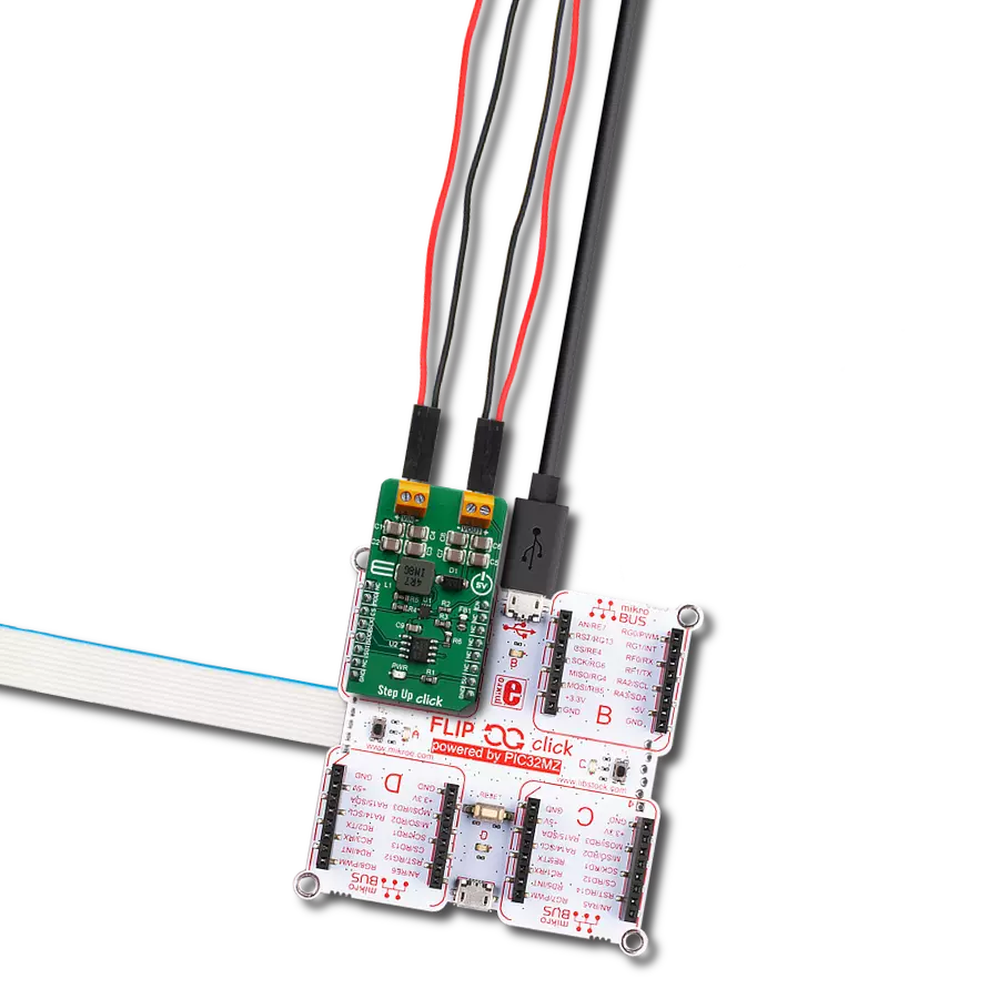
Boost-INV 3 Click
Dev. board
Arduino UNO Rev3
Compiler
NECTO Studio
MCU
ATmega328P
Achieve voltage symmetry effortlessly with our power supply. Where positives and negatives align, our solution stands ready to meet your diverse electrical requirements with precision and ease.
A
A
Hardware Overview
How does it work?
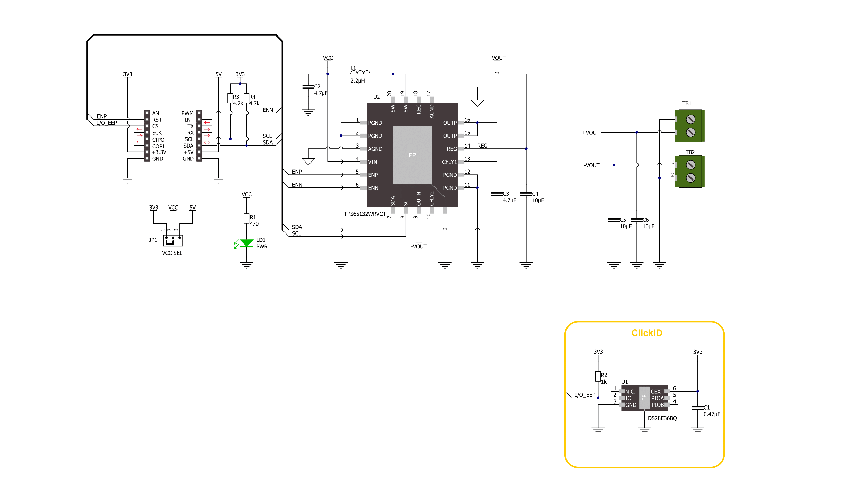
Boost-INV 3 Click is based on the TPS65132, a dual-output power supply from Texas Instruments. The TPS65132 operates with a single inductor scheme to provide high efficiency with a small solution size. The synchronous boost converter generates a positive voltage regulated by an integrated LDO, providing the positive supply rail on the +VOUT terminal. The negative supply rail, available on the -VOUT terminal, is generated by an integrated negative charge pump driven from the boost converter output REG pin. The output voltage is
programmable via an I2C compatible interface, from ±6V to ±4V in 100mV steps with ±5.4V pre-programmed output voltage and a maximum 80mA output current. Both output voltages can be set independently, and their sequencing is also independent. This Click board™ communicates with the host MCU using the standard I2C 2-Wire interface, with a maximum clock frequency in Fast data transfer of up to 400kHz (400kbps). Pulling ENP or ENN pins of the mikroBUS socket to a low logic state turns off either rail (+VOUT or -VOUT,
respectively) and pulling both pins to a low logic state turns off the device entirely (the internal oscillator of the TPS65132 continues running to allow access to the I2C interface). This Click board™ can operate with either 3.3V or 5V logic voltage levels selected via the VCC SEL jumper. This way, both 3.3V and 5V capable MCUs can use the communication lines properly. Also, this Click board™ comes equipped with a library containing easy-to-use functions and an example code that can be used for further development.

Features overview
Development board
Arduino UNO is a versatile microcontroller board built around the ATmega328P chip. It offers extensive connectivity options for various projects, featuring 14 digital input/output pins, six of which are PWM-capable, along with six analog inputs. Its core components include a 16MHz ceramic resonator, a USB connection, a power jack, an
ICSP header, and a reset button, providing everything necessary to power and program the board. The Uno is ready to go, whether connected to a computer via USB or powered by an AC-to-DC adapter or battery. As the first USB Arduino board, it serves as the benchmark for the Arduino platform, with "Uno" symbolizing its status as the
first in a series. This name choice, meaning "one" in Italian, commemorates the launch of Arduino Software (IDE) 1.0. Initially introduced alongside version 1.0 of the Arduino Software (IDE), the Uno has since become the foundational model for subsequent Arduino releases, embodying the platform's evolution.

Microcontroller Overview
MCU Card / MCU

Architecture
AVR
MCU Memory (KB)
32
Silicon Vendor
Microchip
Pin count
28
RAM (Bytes)
2048
You complete me!
Accessories
Click Shield for Arduino UNO has two proprietary mikroBUS™ sockets, allowing all the Click board™ devices to be interfaced with the Arduino UNO board without effort. The Arduino Uno, a microcontroller board based on the ATmega328P, provides an affordable and flexible way for users to try out new concepts and build prototypes with the ATmega328P microcontroller from various combinations of performance, power consumption, and features. The Arduino Uno has 14 digital input/output pins (of which six can be used as PWM outputs), six analog inputs, a 16 MHz ceramic resonator (CSTCE16M0V53-R0), a USB connection, a power jack, an ICSP header, and reset button. Most of the ATmega328P microcontroller pins are brought to the IO pins on the left and right edge of the board, which are then connected to two existing mikroBUS™ sockets. This Click Shield also has several switches that perform functions such as selecting the logic levels of analog signals on mikroBUS™ sockets and selecting logic voltage levels of the mikroBUS™ sockets themselves. Besides, the user is offered the possibility of using any Click board™ with the help of existing bidirectional level-shifting voltage translators, regardless of whether the Click board™ operates at a 3.3V or 5V logic voltage level. Once you connect the Arduino UNO board with our Click Shield for Arduino UNO, you can access hundreds of Click boards™, working with 3.3V or 5V logic voltage levels.

Used MCU Pins
mikroBUS™ mapper
Take a closer look
Click board™ Schematic
Step by step
Project assembly

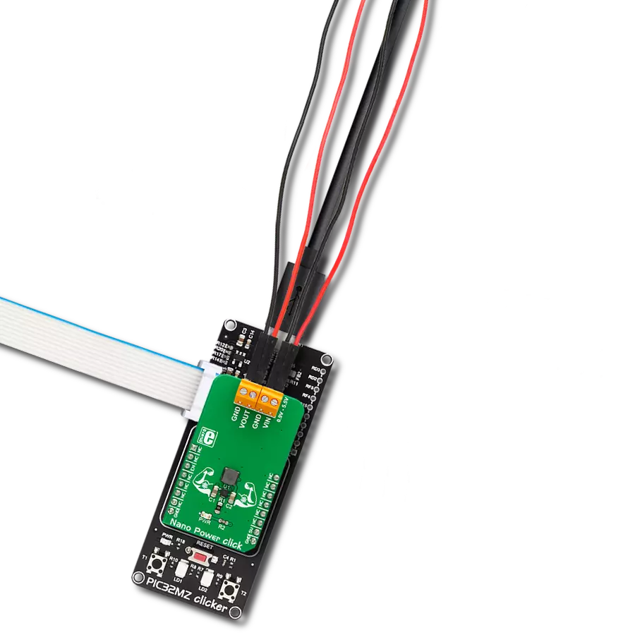
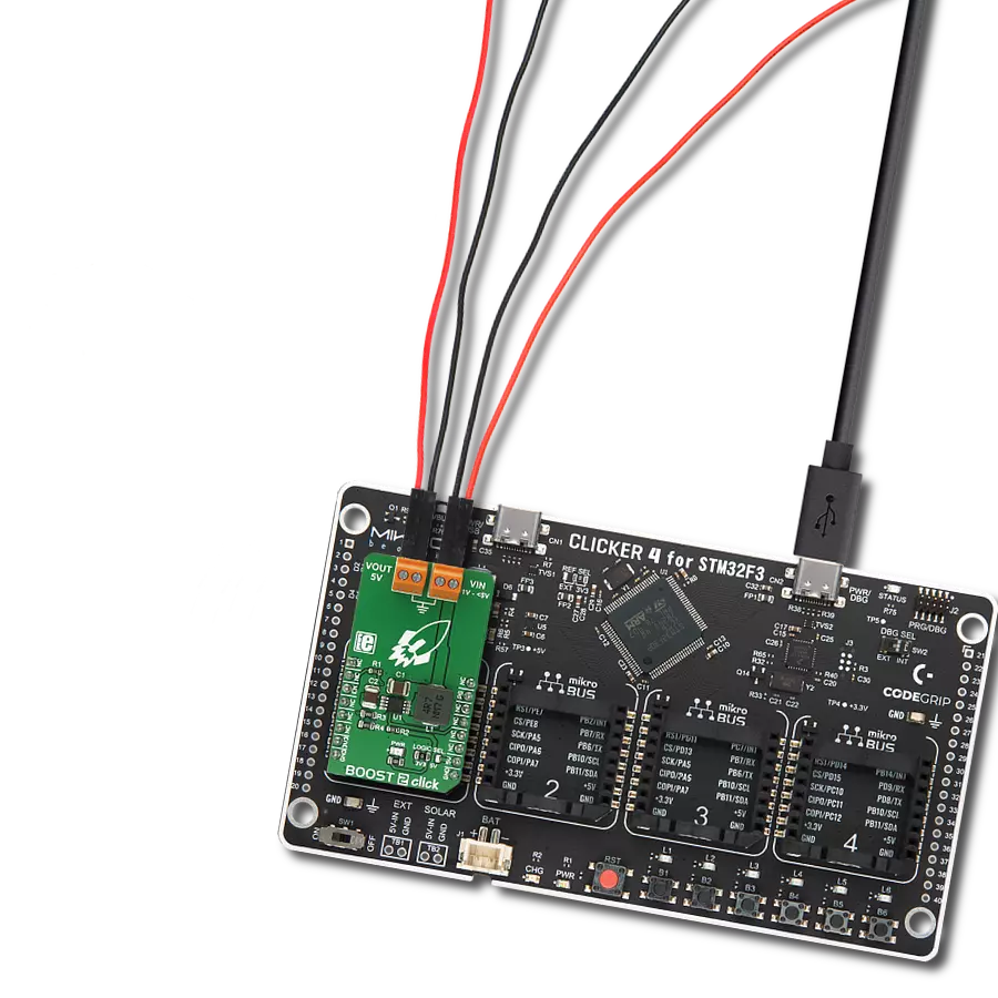
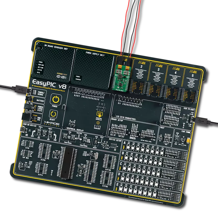
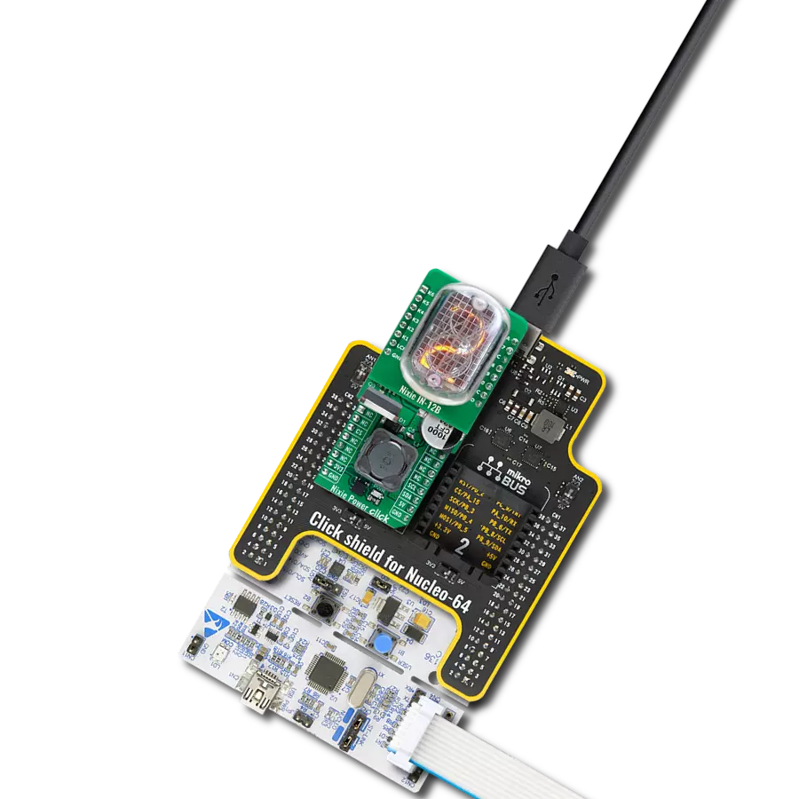
Start by selecting your development board and Click board™. Begin with the Arduino UNO Rev3 as your development board.


Software Support
Library Description
This library contains API for Boost-INV 3 Click driver.
Key functions:
boostinv3_set_enp- Boost-INV 3 set ENP pin state function.boostinv3_set_pos_out- Boost-INV 3 set positive output voltage function.boostinv3_set_neg_out- Boost-INV 3 set negative output voltage function.
Open Source
Code example
The complete application code and a ready-to-use project are available through the NECTO Studio Package Manager for direct installation in the NECTO Studio. The application code can also be found on the MIKROE GitHub account.
/*!
 * @file main.c
 * @brief Boost-INV 3 Click example
 *
 * # Description
 * This library contains API for the Boost-INV 3 Click driver.
 * This driver provides the functions to set the output voltage treshold.
 *
 * The demo application is composed of two sections :
 *
 * ## Application Init
 * Initialization of I2C module and log UART.
 * After driver initialization, default settings enable the positive and
 * negative output and sets the output voltage to 4 V.
 *
 * ## Application Task
 * This example demonstrates the use of the Boost-INV 3 Click board by changing
 * output voltage every 5 seconds starting from 4 V up to 6 V.
 *
 * @author Stefan Ilic
 *
 */

#include "board.h"
#include "log.h"
#include "boostinv3.h"

#define BOOSTINV3_MIN_VOL_LVL           4.0f
#define BOOSTINV3_INCREMENT             0.1f

static boostinv3_t boostinv3;
static log_t logger;

void application_init ( void )
{
    log_cfg_t log_cfg;  /**< Logger config object. */
    boostinv3_cfg_t boostinv3_cfg;  /**< Click config object. */

    /**
     * Logger initialization.
     * Default baud rate: 115200
     * Default log level: LOG_LEVEL_DEBUG
     * @note If USB_UART_RX and USB_UART_TX
     * are defined as HAL_PIN_NC, you will
     * need to define them manually for log to work.
     * See @b LOG_MAP_USB_UART macro definition for detailed explanation.
     */
    LOG_MAP_USB_UART( log_cfg );
    log_init( &logger, &log_cfg );
    log_info( &logger, " Application Init " );

    // Click initialization.
    boostinv3_cfg_setup( &boostinv3_cfg );
    BOOSTINV3_MAP_MIKROBUS( boostinv3_cfg, MIKROBUS_1 );
    if ( I2C_MASTER_ERROR == boostinv3_init( &boostinv3, &boostinv3_cfg ) )
    {
        log_error( &logger, " Communication init." );
        for ( ; ; );
    }
    Delay_ms ( 100 );

    if ( BOOSTINV3_ERROR == boostinv3_default_cfg ( &boostinv3 ) )
    {
        log_error( &logger, " Default configuration." );
        for ( ; ; );
    }

    log_info( &logger, " Application Task " );
}

void application_task ( void )
{
    for ( uint8_t n_cnt = BOOSTINV3_OUT_VOLTAGE_4V; n_cnt <= BOOSTINV3_OUT_VOLTAGE_6V; n_cnt++ )
    {
        err_t error_flag = boostinv3_set_pos_out( &boostinv3, n_cnt );
        error_flag |= boostinv3_set_neg_out( &boostinv3, n_cnt );
        if ( BOOSTINV3_OK == error_flag )
        {
            log_printf( &logger, " Set positive and negative voltage to %.1f V \r\n",
                        ( BOOSTINV3_MIN_VOL_LVL + n_cnt * BOOSTINV3_INCREMENT ) );
        }
        else
        {
            log_printf( &logger, " Error has occurred!!! \r\n" );
        }
        Delay_ms ( 1000 );
        Delay_ms ( 1000 );
        Delay_ms ( 1000 );
        Delay_ms ( 1000 );
        Delay_ms ( 1000 );
    }
}

int main ( void )
{
    /* Do not remove this line or clock might not be set correctly. */
    #ifdef PREINIT_SUPPORTED
    preinit();
    #endif

    application_init( );

    for ( ; ; )
    {
        application_task( );
    }

    return 0;
}

// ------------------------------------------------------------------------ END
Additional Support
Resources
Category:Boost