Voltage boost for superior energy thanks to the MAX17222 and MK64FN1M0VDC12
Get a boost for success

Published Jul 18, 2023
Click board™
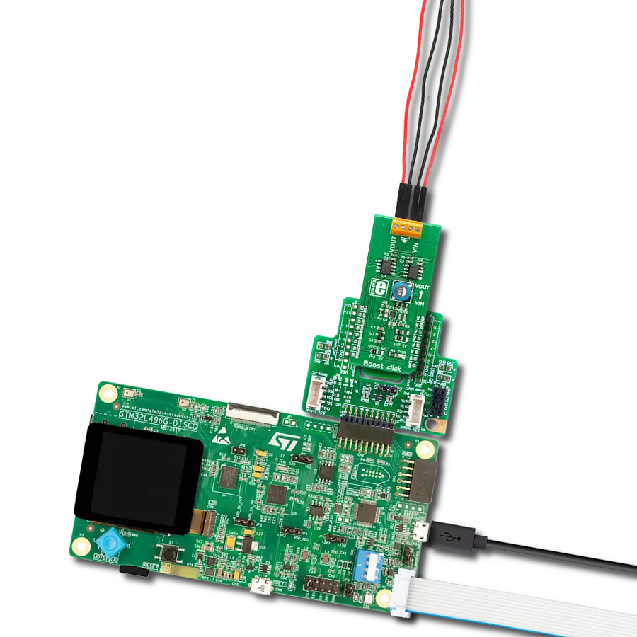
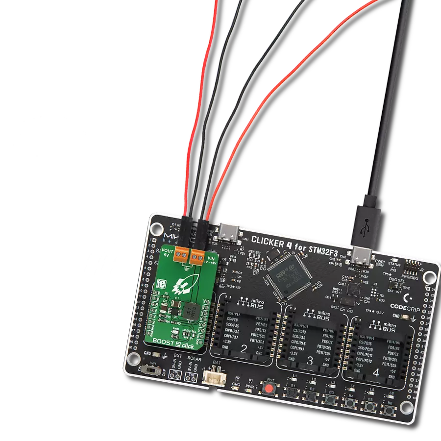
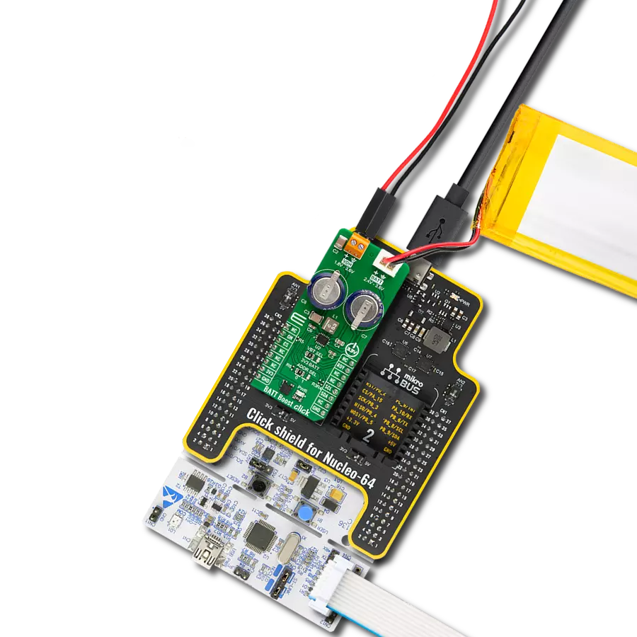
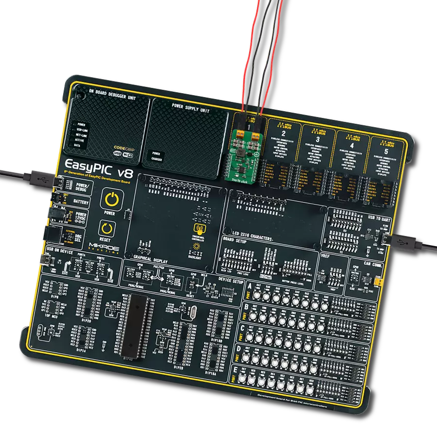
Nano Power Click
Dev. board
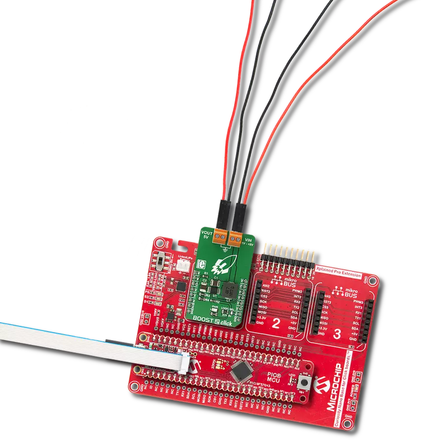
Clicker 2 for Kinetis
Compiler
NECTO Studio
MCU
MK64FN1M0VDC12
Create a boost (step-up) DC-DC converter with extremely high efficiency and low input voltage aimed at the low-power IoT market, battery-powered sensors, and other devices
A
A
Hardware Overview
How does it work?
Nano Power Click is based on the MAX17222, a nano power synchronous boost converter with True Shutdown™ technology, from Analog Devices. The device operates in several modes, allowing optimal utilization of the available power. The device will automatically switch to a different working mode depending on the connected load, providing optimal conditions for a given situation. The MAX17222 uses the pulse frequency modulation control (PFM) topology, which allows high efficiency over a wide range of output currents. The PFM control allows continuous and discontinuous (CCM and DCM) switching modes. Operation of the MAX17222 changes with the connected load, as mentioned above. When the load is very light, the device operates in the Ultra Low Power Mode (ULPM), and the switching is performed in discontinuous mode (DCM). The ULPM is typically used when the device connected at the output is in standby or power-down mode, draining a low current. As the current requirement increases, the MAX17222 device switches to the Low Power mode and further to the High Power mode (LPM and HPM). These modes result in cleaner output and less ripple than the ULPM
mode. When working in HPM, the continuous switching mode (CCM) is used (with no pulses being skipped), providing low noise, ripple-free output voltage, which is suitable for various sensor measurements, A/D conversions, wireless communication, and other noise and ripple-sensitive applications. The EN pin of the MAX17222 is used to enable this device. When a transition from LOW to HIGH logic state appears at this pin (rising edge), it will activate the IC, and regulated 5V will appear at the output (providing the proper input voltage is present). This pin is routed to the mikroBUS™ CS pin, labeled EN. The device will remain enabled, even if the input voltage drops to 0.4V, thanks to the internal ETP section of the MAX17222 IC. Holding the EN pin to a HIGH logic state once the conversion is started results in slightly increased power consumption. The Power LED indicator is connected to the 5V rail of the mikroBUS™ and does not affect the power consumption on the connected external power supply. The power consumption calculations in the datasheet remain true and are not affected by any external components of this Click board™. The Power LED indicates the presence of the
mikroBUS™ voltage, signaling that the EN pin can be controlled via the host MCU. The external power supply can be connected to the input terminals between the VIN and GND, ranging from 0.95V up to 5.5V. However, for an optimal operation of the Nanopower click, the input voltage should be lower than the output voltage. The Nanopower click allows a maximum peak current of 500mA before the current limit protection activates. The output voltage is fixed at 5V by a single resistor, connected between the SEL pin of the IC and GND. This resistor is 0 Ω, and it is basically - an SMD jumper. Using other values (listed in the datasheet of the MAX17222 IC) makes it possible to change the output voltage to a value different than 5V. Please consult the datasheet to select the resistor for the given output voltage properly. The control of the Nanopower click is extremely simple, and it is reduced to controlling a single pin. However, provided library offers functions that simplify and speed up application development even more. The included example application demonstrates their use. This application can be used as a reference for custom projects.

Features overview
Development board
Clicker 2 for Kinetis is a compact starter development board that brings the flexibility of add-on Click boards™ to your favorite microcontroller, making it a perfect starter kit for implementing your ideas. It comes with an onboard 32-bit ARM Cortex-M4F microcontroller, the MK64FN1M0VDC12 from NXP Semiconductors, two mikroBUS™ sockets for Click board™ connectivity, a USB connector, LED indicators, buttons, a JTAG programmer connector, and two 26-pin headers for interfacing with external electronics. Its compact design with clear and easily recognizable silkscreen markings allows you to build gadgets with unique functionalities and
features quickly. Each part of the Clicker 2 for Kinetis development kit contains the components necessary for the most efficient operation of the same board. In addition to the possibility of choosing the Clicker 2 for Kinetis programming method, using a USB HID mikroBootloader or an external mikroProg connector for Kinetis programmer, the Clicker 2 board also includes a clean and regulated power supply module for the development kit. It provides two ways of board-powering; through the USB Micro-B cable, where onboard voltage regulators provide the appropriate voltage levels to each component on the board, or
using a Li-Polymer battery via an onboard battery connector. All communication methods that mikroBUS™ itself supports are on this board, including the well-established mikroBUS™ socket, reset button, and several user-configurable buttons and LED indicators. Clicker 2 for Kinetis is an integral part of the Mikroe ecosystem, allowing you to create a new application in minutes. Natively supported by Mikroe software tools, it covers many aspects of prototyping thanks to a considerable number of different Click boards™ (over a thousand boards), the number of which is growing every day.

Microcontroller Overview
MCU Card / MCU

Architecture
ARM Cortex-M4
MCU Memory (KB)
1024
Silicon Vendor
NXP
Pin count
121
RAM (Bytes)
262144
Used MCU Pins
mikroBUS™ mapper
Take a closer look
Click board™ Schematic

Step by step
Project assembly

Start by selecting your development board and Click board™. Begin with the Clicker 2 for Kinetis as your development board.


Track your results in real time
Application Output
1. Application Output - In Debug mode, the 'Application Output' window enables real-time data monitoring, offering direct insight into execution results. Ensure proper data display by configuring the environment correctly using the provided tutorial.

2. UART Terminal - Use the UART Terminal to monitor data transmission via a USB to UART converter, allowing direct communication between the Click board™ and your development system. Configure the baud rate and other serial settings according to your project's requirements to ensure proper functionality. For step-by-step setup instructions, refer to the provided tutorial.

3. Plot Output - The Plot feature offers a powerful way to visualize real-time sensor data, enabling trend analysis, debugging, and comparison of multiple data points. To set it up correctly, follow the provided tutorial, which includes a step-by-step example of using the Plot feature to display Click board™ readings. To use the Plot feature in your code, use the function: plot(*insert_graph_name*, variable_name);. This is a general format, and it is up to the user to replace 'insert_graph_name' with the actual graph name and 'variable_name' with the parameter to be displayed.

Software Support
Library Description
This library contains API for Nano Power Click driver.
Key functions:
nanopw_enable_device- This function enables and disables the device
Open Source
Code example
The complete application code and a ready-to-use project are available through the NECTO Studio Package Manager for direct installation in the NECTO Studio. The application code can also be found on the MIKROE GitHub account.
/*!
 * \file
 * \brief Nano Power Click example
 *
 * # Description
 * This aplication performs control of the device's voltage.
 *
 * The demo application is composed of two sections :
 *
 * ## Application Init
 * Initializes GPIO driver.
 *
 * ## Application Task
 * Turns device on for 5 seconds and than turns device off for 10 seconds,
 * then the output voltage starts to fall.
 * When input voltage rises from 0.8V to 5.5V,
 * the output voltage rises from 5.1V to 5.25V.
 * When input voltage is less than 0.8V, the output voltage is less than 5V.
 *
 *
 * \author Petar Suknjaja
 *
 */
// ------------------------------------------------------------------- INCLUDES

#include "board.h"
#include "log.h"
#include "nanopower.h"

// ------------------------------------------------------------------ VARIABLES

static nanopower_t nanopower;
static log_t logger;

// ------------------------------------------------------ APPLICATION FUNCTIONS

void application_init ( void )
{
    log_cfg_t log_cfg;
    nanopower_cfg_t cfg;

    /**
     * Logger initialization.
     * Default baud rate: 115200
     * Default log level: LOG_LEVEL_DEBUG
     * @note If USB_UART_RX and USB_UART_TX
     * are defined as HAL_PIN_NC, you will
     * need to define them manually for log to work.
     * See @b LOG_MAP_USB_UART macro definition for detailed explanation.
     */
    LOG_MAP_USB_UART( log_cfg );
    log_init( &logger, &log_cfg );
    log_info(&logger, "---- Application Init ----");

    //  Click initialization.

    nanopower_cfg_setup( &cfg );
    NANOPOWER_MAP_MIKROBUS( cfg, MIKROBUS_1 );
    nanopower_init( &nanopower, &cfg );
}

void application_task ( void )
{
    log_printf(&logger,"Device enabled\r\n");
    nanopw_enable_device( &nanopower, NANOPW_ENABLE_DEVICE );
    Delay_ms ( 1000 );
    Delay_ms ( 1000 );
    Delay_ms ( 1000 );
    Delay_ms ( 1000 );
    Delay_ms ( 1000 );
    log_printf(&logger,"Device disabled\r\n");
    nanopw_enable_device( &nanopower, NANOPW_DISABLE_DEVICE );
    // 10 seconds delay
    Delay_ms ( 1000 );
    Delay_ms ( 1000 );
    Delay_ms ( 1000 );
    Delay_ms ( 1000 );
    Delay_ms ( 1000 );
    Delay_ms ( 1000 );
    Delay_ms ( 1000 );
    Delay_ms ( 1000 );
    Delay_ms ( 1000 );
    Delay_ms ( 1000 );
}

int main ( void )
{
    /* Do not remove this line or clock might not be set correctly. */
    #ifdef PREINIT_SUPPORTED
    preinit();
    #endif

    application_init( );

    for ( ; ; )
    {
        application_task( );
    }

    return 0;
}


// ------------------------------------------------------------------------ END