Discover the magic of step-down buck conversion with MAX17506 and ATmega328
Step down, Amp up!
Published Feb 14, 2024
Click board™
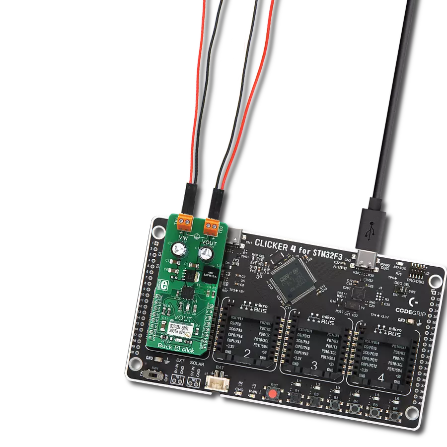
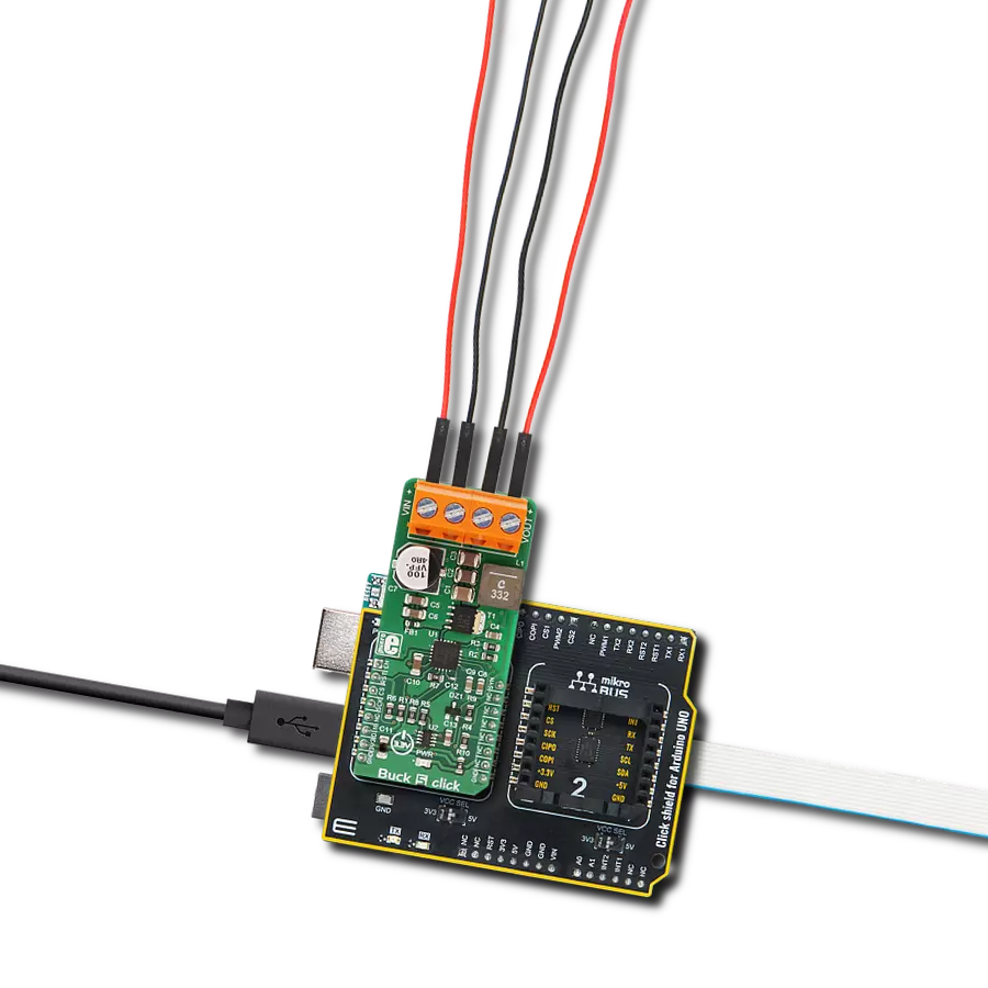
Buck 5 Click
Dev. board
Arduino UNO Rev3
Compiler
NECTO Studio
MCU
ATmega328
Designed to lower the input voltage while maintaining stable performance efficiently, our converter empowers your gadgets with optimal power management
A
A
Hardware Overview
How does it work?
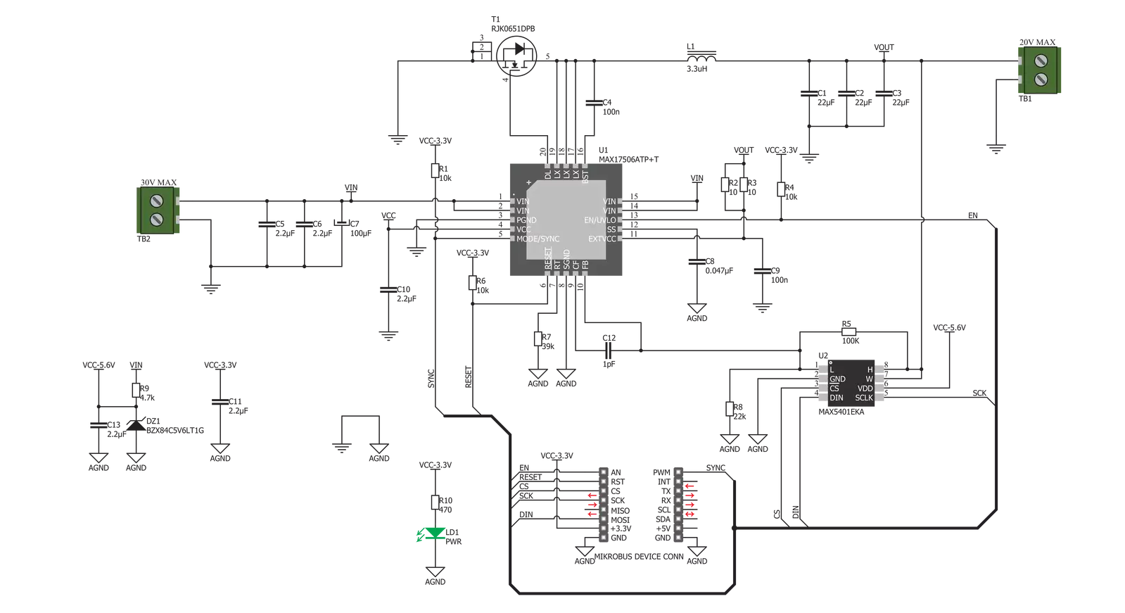
Buck 5 Click is equipped with the MAX17506, a high-efficiency, synchronous step-down DC/DC converter with internal compensation from Analog Devices. This advanced step-down converter IC with an integrated high-side MOSFET requires a minimum number of external components, thanks to the internal feedback loop compensation. It utilizes a peak-current-mode control architecture. While the high side MOSFET is open and the current through the inductor ramps up, an overcurrent event will cause the MOSFET to close, preventing this current from becoming dangerously high. If there is a short circuit condition on the output, the device will reattempt to start after a timeout period, and if the condition is still present at the output, it will be turned off for another timeout period. The MAX5401, a 256-tap digital potentiometer with an SPI Interface made by Analog Devices, is used on the feedback loop to allow adjustment of the output voltage via the SPI interface. It is used in place of the fixed voltage divider found on the reference design of the MAX17506, regulating the output voltage to a programmed value that way. As a result, sending a digital value through the SPI interface to the MAX5401 makes it possible to control the output voltage level in the range from 0.9V to 5.5V. While operating normally (PWM
mode), the high and the low side MOSFETs are switched synchronously with the signal from the internal PWM generator, causing the current through the inductor to ramp up and down, regulating the output voltage that way. The PWM signal's lower pulse width (duty cycle) results in a lower voltage at the output. The low-side MOSFET is placed outside the IC, allowing less DC/DC converter IC dissipation. Besides the PWM mode, the device can also operate in the PFM mode (Pulse Frequency Modulation). This mode allows even higher efficiency for light loads, as the low-side MOSFET is completely unused. The high side MOSFET charges the inductor, letting the load drain it. During this period, the IC is in a hibernation state. This mode results in slightly more ripple at the output, with the added benefit of high efficiency for light loads. It is perfectly suited to power devices in the low power consumption mode (Sleep, Standby, and more). The DCM mode is the compromise mode between PWM and PFM modes. The low-side MOSFET is still unused for light loads, but the PWM pulses are not skipped, and the IC constantly drives the high-side MOSFET. This mode produces ripple at the output, but it is slightly less efficient than the PFM mode for light loads. The MODE/SYNC pin selects different modes. The IC is set to work in DCM
mode with the pull-up resistor by default. The MODE/SYNC pin of the IC is routed to the mikroBUS™ PWM pin (labeled as SYN), allowing the MCU to control the mode. When this pin is set to a LOW logic level, the constant frequency PWM mode is set. The same pin (MODE/SYNC) can synchronize the converter IC (fs) switching frequency when needed. The 39K resistor determines this frequency to about 480 kHz. However, the frequency can be synchronized with an external source from 1.1 x fs to 1.4 x fs. The #RESET pin of the IC is routed to the mikroBUS™ RST pin. This pin signalizes problems with the output voltage. The pin is driven to a LOW logic level when the output voltage drops under 92% of the nominal value or during the thermal shutdown. It is an open drain output, otherwise pulled to a HIGH logic level (when not asserted). To enable the buck converter IC, a HIGH logic level needs to be present at the EN pin of the IC, routed to the mikroBUS™ AN pin (labeled as EN). This allows the MCU to control the Power ON function of the Click board™ effectively. When the IC is enabled, the LED indicator labeled EN indicates that the IC is activated and the step-down conversion is in progress. The soft-start circuit prevents high inrush currents by ramping up the output voltage from 0V to the nominal value.

Features overview
Development board
Arduino UNO is a versatile microcontroller board built around the ATmega328P chip. It offers extensive connectivity options for various projects, featuring 14 digital input/output pins, six of which are PWM-capable, along with six analog inputs. Its core components include a 16MHz ceramic resonator, a USB connection, a power jack, an
ICSP header, and a reset button, providing everything necessary to power and program the board. The Uno is ready to go, whether connected to a computer via USB or powered by an AC-to-DC adapter or battery. As the first USB Arduino board, it serves as the benchmark for the Arduino platform, with "Uno" symbolizing its status as the
first in a series. This name choice, meaning "one" in Italian, commemorates the launch of Arduino Software (IDE) 1.0. Initially introduced alongside version 1.0 of the Arduino Software (IDE), the Uno has since become the foundational model for subsequent Arduino releases, embodying the platform's evolution.

Microcontroller Overview
MCU Card / MCU
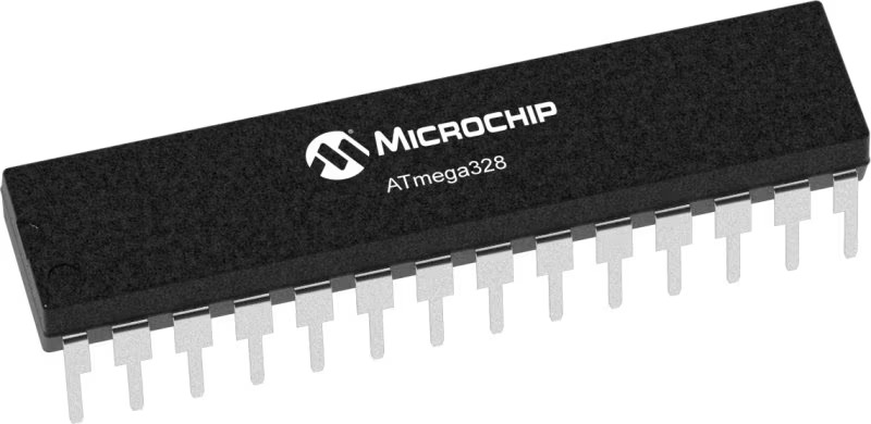
Architecture
AVR
MCU Memory (KB)
32
Silicon Vendor
Microchip
Pin count
32
RAM (Bytes)
2048
You complete me!
Accessories
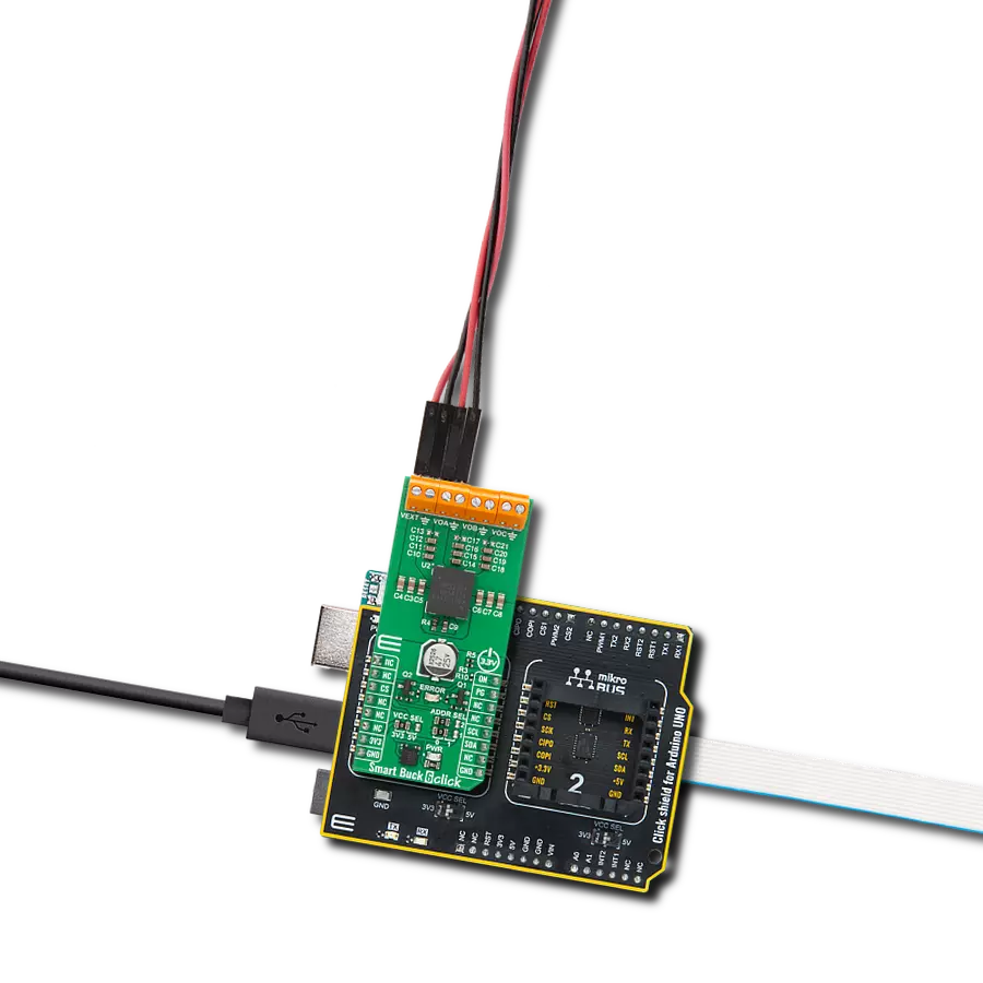
Click Shield for Arduino UNO has two proprietary mikroBUS™ sockets, allowing all the Click board™ devices to be interfaced with the Arduino UNO board without effort. The Arduino Uno, a microcontroller board based on the ATmega328P, provides an affordable and flexible way for users to try out new concepts and build prototypes with the ATmega328P microcontroller from various combinations of performance, power consumption, and features. The Arduino Uno has 14 digital input/output pins (of which six can be used as PWM outputs), six analog inputs, a 16 MHz ceramic resonator (CSTCE16M0V53-R0), a USB connection, a power jack, an ICSP header, and reset button. Most of the ATmega328P microcontroller pins are brought to the IO pins on the left and right edge of the board, which are then connected to two existing mikroBUS™ sockets. This Click Shield also has several switches that perform functions such as selecting the logic levels of analog signals on mikroBUS™ sockets and selecting logic voltage levels of the mikroBUS™ sockets themselves. Besides, the user is offered the possibility of using any Click board™ with the help of existing bidirectional level-shifting voltage translators, regardless of whether the Click board™ operates at a 3.3V or 5V logic voltage level. Once you connect the Arduino UNO board with our Click Shield for Arduino UNO, you can access hundreds of Click boards™, working with 3.3V or 5V logic voltage levels.

Used MCU Pins
mikroBUS™ mapper
Take a closer look
Click board™ Schematic
Step by step
Project assembly

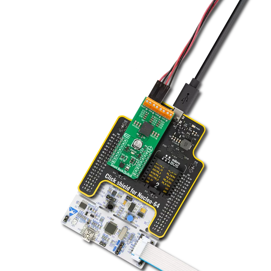
Start by selecting your development board and Click board™. Begin with the Arduino UNO Rev3 as your development board.


Software Support
Library Description
This library contains API for Buck 5 Click driver.
Key functions:
buck5_power_on- This function wake up the chipbuck5_reset- This function reset the chipbuck5_set_output_voltage- Maximum output voltage is 5.5V (255 set value), and minimum output voltage is 1V (0 set value)
Open Source
Code example
The complete application code and a ready-to-use project are available through the NECTO Studio Package Manager for direct installation in the NECTO Studio. The application code can also be found on the MIKROE GitHub account.
/*!
 * \file
 * \brief Buck5 Click example
 *
 * # Description
 * Buck 5 Click is a high-efficiency buck DC/DC converter, which can provide digitally
 * adjusted step-down voltage on its output while delivering a considerable amount of current.
 * Buck 5 Click accepts a wide voltage range on its input - from 5V to 30V. The output voltage
 * may be adjusted via the SPI interface, in the range from 0.9V to approximately 5.5V.
 *
 * The demo application is composed of two sections :
 *
 * ## Application Init
 * Initializes driver init, and enables the Click board.
 *
 * ## Application Task
 * Increases the output voltage by 500mV every 3 seconds from MIN to MAX VOUT.
 *
 * \author MikroE Team
 *
 */
// ------------------------------------------------------------------- INCLUDES

#include "board.h"
#include "log.h"
#include "buck5.h"

// ------------------------------------------------------------------ VARIABLES

static buck5_t buck5;
static log_t logger;

// ------------------------------------------------------ APPLICATION FUNCTIONS

void application_init ( void )
{
    log_cfg_t log_cfg;
    buck5_cfg_t cfg;

    /**
     * Logger initialization.
     * Default baud rate: 115200
     * Default log level: LOG_LEVEL_DEBUG
     * @note If USB_UART_RX and USB_UART_TX
     * are defined as HAL_PIN_NC, you will
     * need to define them manually for log to work.
     * See @b LOG_MAP_USB_UART macro definition for detailed explanation.
     */
    LOG_MAP_USB_UART( log_cfg );
    log_init( &logger, &log_cfg );
    log_info( &logger, "---- Application Init ----" );

    //  Click initialization.

    buck5_cfg_setup( &cfg );
    BUCK5_MAP_MIKROBUS( cfg, MIKROBUS_1 );
    buck5_init( &buck5, &cfg );

    buck5_power_on( &buck5 );
    buck5_reset( &buck5 );
}

void application_task ( void )
{
    buck5_set_output_voltage( &buck5, BUCK5_VOLTAGE_MIN );
    log_printf( &logger, "VOUT: MIN\r\n" );
    Delay_ms ( 1000 );
    Delay_ms ( 1000 );
    Delay_ms ( 1000 );
    buck5_set_output_voltage( &buck5, BUCK5_VOLTAGE_1000mV );
    log_printf( &logger, "VOUT: ~1V\r\n" );
    Delay_ms ( 1000 );
    Delay_ms ( 1000 );
    Delay_ms ( 1000 );
    buck5_set_output_voltage( &buck5, BUCK5_VOLTAGE_1500mV );
    log_printf( &logger, "VOUT: ~1.5V\r\n" );
    Delay_ms ( 1000 );
    Delay_ms ( 1000 );
    Delay_ms ( 1000 );
    buck5_set_output_voltage( &buck5, BUCK5_VOLTAGE_2000mV );
    log_printf( &logger, "VOUT: ~2V\r\n" );
    Delay_ms ( 1000 );
    Delay_ms ( 1000 );
    Delay_ms ( 1000 );
    buck5_set_output_voltage( &buck5, BUCK5_VOLTAGE_2500mV );
    log_printf( &logger, "VOUT: ~2.5V\r\n" );
    Delay_ms ( 1000 );
    Delay_ms ( 1000 );
    Delay_ms ( 1000 );
    buck5_set_output_voltage( &buck5, BUCK5_VOLTAGE_3000mV );
    log_printf( &logger, "VOUT: ~3V\r\n" );
    Delay_ms ( 1000 );
    Delay_ms ( 1000 );
    Delay_ms ( 1000 );
    buck5_set_output_voltage( &buck5, BUCK5_VOLTAGE_3500mV );
    log_printf( &logger, "VOUT: ~3.5V\r\n" );
    Delay_ms ( 1000 );
    Delay_ms ( 1000 );
    Delay_ms ( 1000 );
    buck5_set_output_voltage( &buck5, BUCK5_VOLTAGE_4000mV );
    log_printf( &logger, "VOUT: ~4V\r\n" );
    Delay_ms ( 1000 );
    Delay_ms ( 1000 );
    Delay_ms ( 1000 );
    buck5_set_output_voltage( &buck5, BUCK5_VOLTAGE_4500mV );
    log_printf( &logger, "VOUT: ~4.5V\r\n" );
    Delay_ms ( 1000 );
    Delay_ms ( 1000 );
    Delay_ms ( 1000 );
    buck5_set_output_voltage( &buck5, BUCK5_VOLTAGE_5000mV );
    log_printf( &logger, "VOUT: ~5V\r\n" );
    Delay_ms ( 1000 );
    Delay_ms ( 1000 );
    Delay_ms ( 1000 );
    buck5_set_output_voltage( &buck5, BUCK5_VOLTAGE_MAX );
    log_printf( &logger, "VOUT: MAX\r\n" );
    Delay_ms ( 1000 );
    Delay_ms ( 1000 );
    Delay_ms ( 1000 );
}

int main ( void )
{
    /* Do not remove this line or clock might not be set correctly. */
    #ifdef PREINIT_SUPPORTED
    preinit();
    #endif

    application_init( );

    for ( ; ; )
    {
        application_task( );
    }

    return 0;
}


// ------------------------------------------------------------------------ END
Additional Support
Resources
Category:Buck