Create precise time intervals with DS1087L and ATmega328P
Accurate square wave generator

Published Feb 14, 2024
Click board™
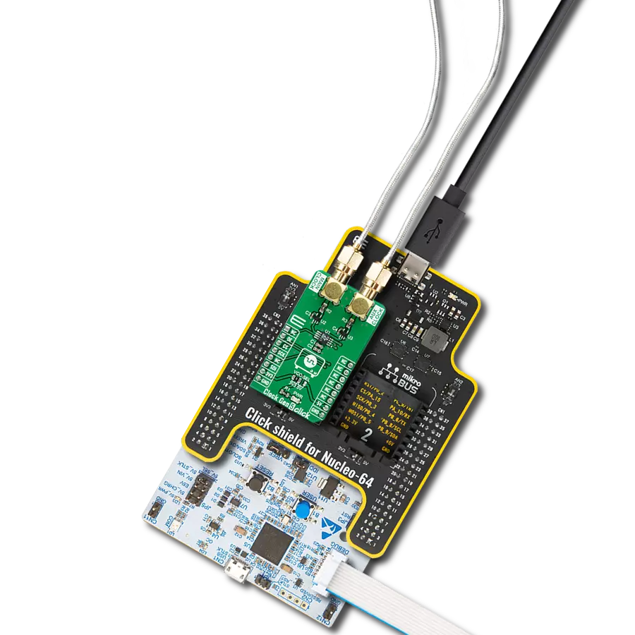
Clock Gen 2 Click
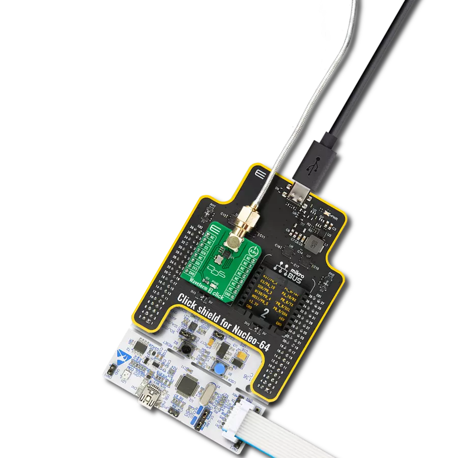
Dev. board
Arduino UNO Rev3
Compiler
NECTO Studio
MCU
ATmega328P
Elevate your engineering solution with a cutting-edge clock generator, delivering reliable and efficient timing signals
A
A
Hardware Overview
How does it work?
Clock Gen 2 Click is based on the DS1087, a 3.3V spread-spectrum EconOscillator from Analog Devices. This IC is factory-produced with a range of different master clock frequencies, ranging from 33.3 MHz, up to 66.6 MHz, with variable spread spectrum percentages. The IC on the Clock Gen 2 click has the master clock fixed to 66.6 MHz, allowing the frequency range from 260 kHz to 66.6 MHz. This IC uses the clock prescaler from 2 0 to 2 8 to achieve frequencies different from the master frequency. By selecting the spread-spectrum percentage, it is possible to avoid the generation of too much EMI, which otherwise might violate the FCC/IEC regulations. As mentioned, the internal clock frequency that the DS1087 generates is 66.6MHz. The master clock is frequency-modulated by the internal triangle wave generator. The main oscillator frequency can be dithered below the maximum frequency by a selectable ratio. A bit in the prescaler register determines the spread-spectrum dither range, which can be selected between 2% and 4%
under the main clock frequency. The IC pin labeled as SPRD is routed to the mikroBUS™ PWM pin. A logic HIGH level on this pin enables the spread-spectrum function. The DS1087LU is equipped with non-volatile memory locations (EEPROM) to store the content of all the configuration registers. Writing data to the configuration registers can be automatically mirrored to the EEPROM. This is controlled by the Write Control bit (WC). It allows automatically storing data to EEPROM after each register change (WC = 0, default) or storing the config data manually by issuing the WRITE EE command (WC = 1). This feature allows the configuration to be remembered between the POR (Power ON Reset) cycles. The output Enable (OE) pin allows the output clock to be turned off at the output pin. A logic HIGH level on this pin turns off the clock output. However, this will not turn off the internal master clock generator, so the IC will still drain the power necessary to work. To completely put the device in a power-down mode, another pin is
used: a logic LOW level on the PDN pin shuts down the master oscillator, draining less current from the power source. The OE pin is routed to the mikroBUS™ CS pin and is labeled as OE, while the PDN pin is routed to the RST pin of the mikroBUS™ and is labeled as PDN. These signals are synchronized with the internal master clock, preventing glitches at the output. The clock output signal is at the SMA connector on the Click board™. This connector protects the high-frequency clock signal and further reduces EMI. It also provides reliable contact with the least possible losses. The clock output signal amplitude is 2.4V, which makes this Click board™ usable with most 3.3V operated MCUs and other devices. The standardized I2C interface allows this Click board™ to be interfaced with a wide range of devices. I2C clock and data pins of the IC (SCL and SDA) are routed to the appropriate mikroBUS™ pins, allowing simple and reliable interfacing.


Features overview
Development board
Arduino UNO is a versatile microcontroller board built around the ATmega328P chip. It offers extensive connectivity options for various projects, featuring 14 digital input/output pins, six of which are PWM-capable, along with six analog inputs. Its core components include a 16MHz ceramic resonator, a USB connection, a power jack, an
ICSP header, and a reset button, providing everything necessary to power and program the board. The Uno is ready to go, whether connected to a computer via USB or powered by an AC-to-DC adapter or battery. As the first USB Arduino board, it serves as the benchmark for the Arduino platform, with "Uno" symbolizing its status as the
first in a series. This name choice, meaning "one" in Italian, commemorates the launch of Arduino Software (IDE) 1.0. Initially introduced alongside version 1.0 of the Arduino Software (IDE), the Uno has since become the foundational model for subsequent Arduino releases, embodying the platform's evolution.

Microcontroller Overview
MCU Card / MCU

Architecture
AVR
MCU Memory (KB)
32
Silicon Vendor
Microchip
Pin count
28
RAM (Bytes)
2048
You complete me!
Accessories
Click Shield for Arduino UNO has two proprietary mikroBUS™ sockets, allowing all the Click board™ devices to be interfaced with the Arduino UNO board without effort. The Arduino Uno, a microcontroller board based on the ATmega328P, provides an affordable and flexible way for users to try out new concepts and build prototypes with the ATmega328P microcontroller from various combinations of performance, power consumption, and features. The Arduino Uno has 14 digital input/output pins (of which six can be used as PWM outputs), six analog inputs, a 16 MHz ceramic resonator (CSTCE16M0V53-R0), a USB connection, a power jack, an ICSP header, and reset button. Most of the ATmega328P microcontroller pins are brought to the IO pins on the left and right edge of the board, which are then connected to two existing mikroBUS™ sockets. This Click Shield also has several switches that perform functions such as selecting the logic levels of analog signals on mikroBUS™ sockets and selecting logic voltage levels of the mikroBUS™ sockets themselves. Besides, the user is offered the possibility of using any Click board™ with the help of existing bidirectional level-shifting voltage translators, regardless of whether the Click board™ operates at a 3.3V or 5V logic voltage level. Once you connect the Arduino UNO board with our Click Shield for Arduino UNO, you can access hundreds of Click boards™, working with 3.3V or 5V logic voltage levels.

Used MCU Pins
mikroBUS™ mapper
Take a closer look
Click board™ Schematic

Step by step
Project assembly

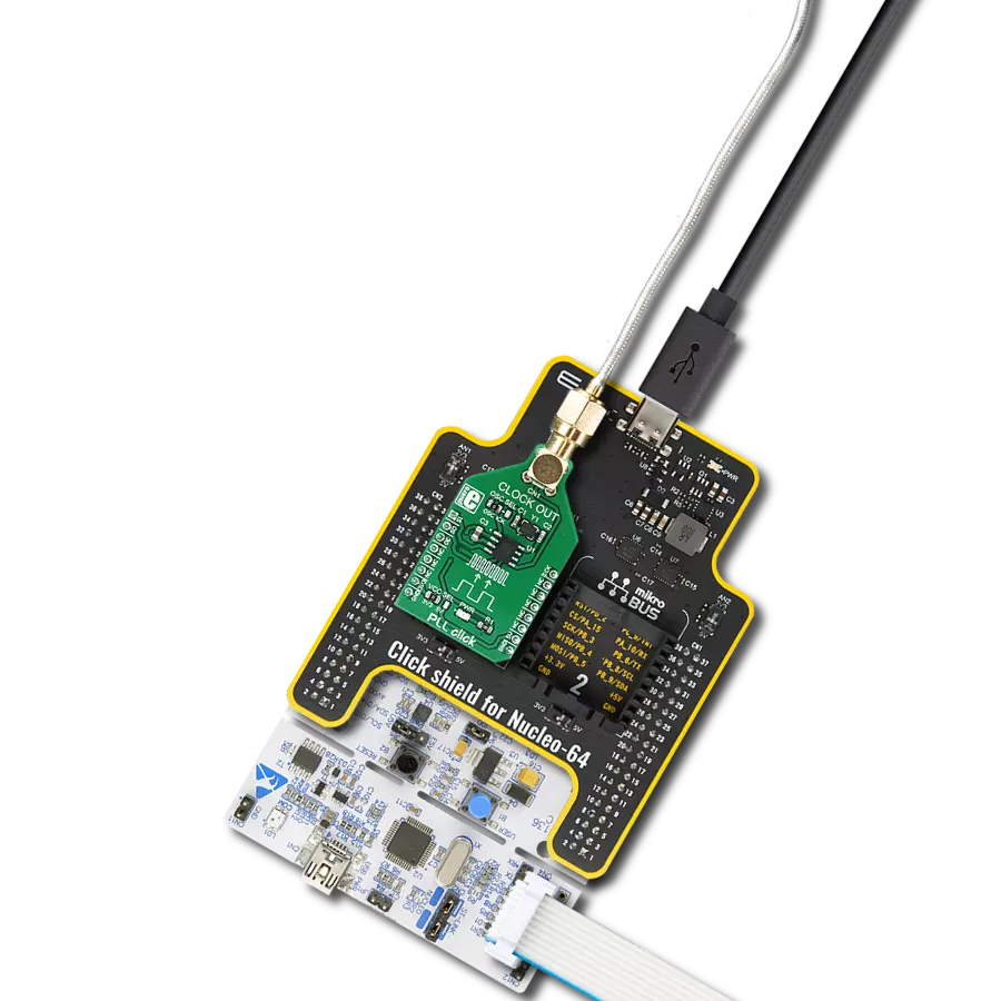
Start by selecting your development board and Click board™. Begin with the Arduino UNO Rev3 as your development board.


Software Support
Library Description
This library contains API for Clock Gen 2 Click driver.
Key functions:
clockgen2_output_enable- Function for enabling/disabling of the clock outputclockgen2_auto_setting_preserve- Function used for enabling/disabling auto settings preservationclockgen2_set_prescaler- Function for setting the main clock prescaler
Open Source
Code example
The complete application code and a ready-to-use project are available through the NECTO Studio Package Manager for direct installation in the NECTO Studio. The application code can also be found on the MIKROE GitHub account.
/*!
 * \file
 * \brief ClockGen2 Click example
 *
 * # Description
 * This application enables generation of square waved clock signal in range from 260 kHz to 66,6 MHz
 *
 * The demo application is composed of two sections :
 *
 * ## Application Init
 * Driver initialization.
 *
 * ## Application Task
 * Changes the prescaler and enables/disables the clock output.
 *
 *
 * \author MikroE Team
 *
 */
// ------------------------------------------------------------------- INCLUDES

#include "board.h"
#include "log.h"
#include "clockgen2.h"

// ------------------------------------------------------------------ VARIABLES

static clockgen2_t clockgen2;
static log_t logger;

// ------------------------------------------------------ APPLICATION FUNCTIONS

void application_init ( void )
{
    log_cfg_t log_cfg;
    clockgen2_cfg_t cfg;

    /**
     * Logger initialization.
     * Default baud rate: 115200
     * Default log level: LOG_LEVEL_DEBUG
     * @note If USB_UART_RX and USB_UART_TX
     * are defined as HAL_PIN_NC, you will
     * need to define them manually for log to work.
     * See @b LOG_MAP_USB_UART macro definition for detailed explanation.
     */
    LOG_MAP_USB_UART( log_cfg );
    log_init( &logger, &log_cfg );
    log_info( &logger, "---- Application Init ----" );

    //  Click initialization.

    clockgen2_cfg_setup( &cfg );
    CLOCKGEN2_MAP_MIKROBUS( cfg, MIKROBUS_1 );
    clockgen2_init( &clockgen2, &cfg );

    Delay_ms ( 100 );
}

void application_task ( void )
{
    //  Task implementation.

    char i;

     for ( i = 5; i< 8; i++ )
     {
       clockgen2_set_prescaler( &clockgen2, i );
       clockgen2_output_enable( &clockgen2, 1 );
       Delay_ms ( 1000 );
       Delay_ms ( 1000 );

       clockgen2_output_enable( &clockgen2, 0 );
       Delay_ms ( 1000 );
       Delay_ms ( 1000 );
     }
}

int main ( void )
{
    /* Do not remove this line or clock might not be set correctly. */
    #ifdef PREINIT_SUPPORTED
    preinit();
    #endif

    application_init( );

    for ( ; ; )
    {
        application_task( );
    }

    return 0;
}


// ------------------------------------------------------------------------ END
Additional Support
Resources
Category:Clock generator