Decode, express, and amplify data across diverse applications with MCP4728 and ATmega328P
Empower data expression
Published Feb 14, 2024
Click board™
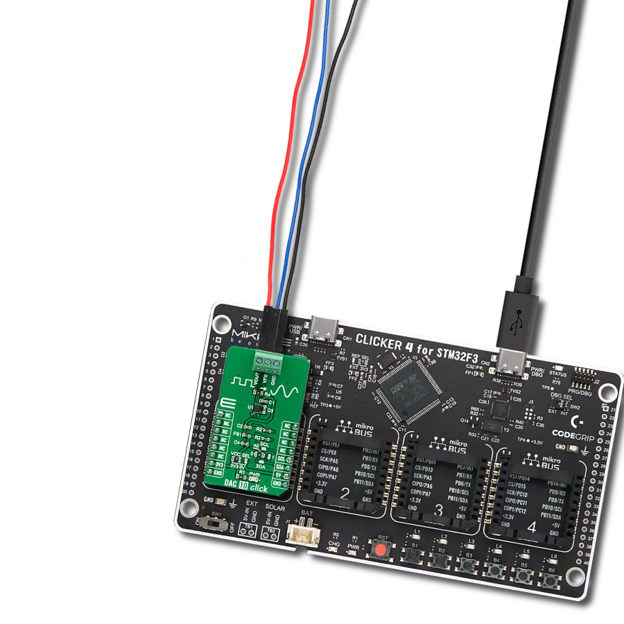
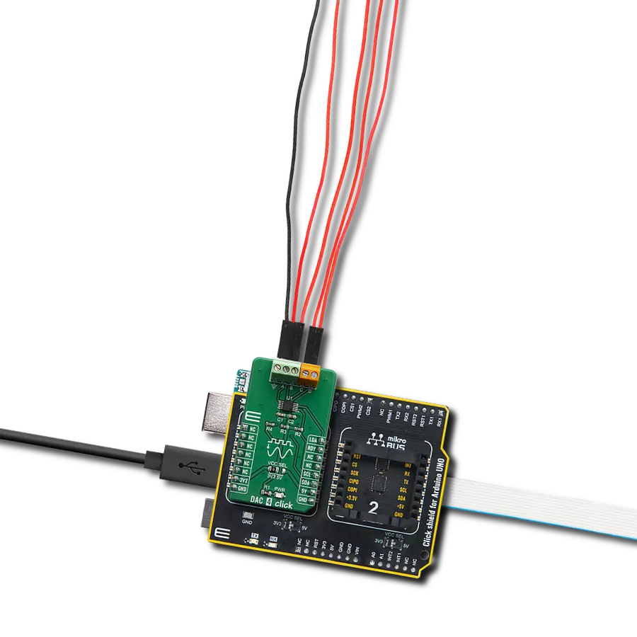
DAC 4 Click
Dev. board
Arduino UNO Rev3
Compiler
NECTO Studio
MCU
ATmega328P
Designed for precision, it transforms digital insights into analog realities, enabling seamless communication and decision-making
A
A
Hardware Overview
How does it work?
DAC 4 Click is based on the MCP4728, a quad, 12-bit voltage output Digital-to-Analog converter (DAC) with nonvolatile memory (EEPROM) from Microchip. Its onboard precision output amplifier allows it to achieve rail-to-rail analog output swing. The DAC input codes, device configuration bits, and I2C address bits are programmable to the nonvolatile memory (EEPROM) using I2C serial interface commands. The nonvolatile memory feature enables the DAC device to hold the DAC input codes during power-off time, allowing the DAC outputs to be available immediately after power-up with the saved settings. The MCP4728 device has a high-precision internal voltage reference (VREF = 2.048V). The user can select the internal reference, or an external reference may be used (VDD) for each channel individually. This
gives the ADC 4-click good flexibility for use in various applications. Each channel can be operated individually in Normal mode or Power-Down mode by setting the configuration register bits. In Power-Down mode, most of the internal circuits in the powered-down channel are turned off for power savings, and the output amplifier can be configured to present a known low, medium, or high resistance output load. This device also includes a Power-on Reset (POR) circuit to ensure reliable power-up and an onboard charge pump for the EEPROM programming voltage. The MCP4728 has four output pins routed to the output terminal blocks (TB1 and TB2). The output range of the DAC is 0 V to VREF or 0 V to 2×V REF. The communication with the main MCU is established over a two-wire I2C compatible serial
interface, with standard (100 kHz), fast (400 kHz), or high speed (3.4 MHz) modes supported. The I2C lines (SCL and SDA) are routed to the dedicated mikroBUS™pins. The LDA pin is a multipurpose GPIO: It can be used as Synchronization input or for the device I2C address selection. RDY pin can also optionally be used to monitor the status of EEPROM programming activity. This Click board™ can operate with either 3.3V or 5V logic voltage levels selected via the VCC SEL jumper. This way, both 3.3V and 5V capable MCUs can use the communication lines properly. Also, this Click board™ comes equipped with a library containing easy-to-use functions and an example code that can be used, as a reference, for further development.


Features overview
Development board
Arduino UNO is a versatile microcontroller board built around the ATmega328P chip. It offers extensive connectivity options for various projects, featuring 14 digital input/output pins, six of which are PWM-capable, along with six analog inputs. Its core components include a 16MHz ceramic resonator, a USB connection, a power jack, an
ICSP header, and a reset button, providing everything necessary to power and program the board. The Uno is ready to go, whether connected to a computer via USB or powered by an AC-to-DC adapter or battery. As the first USB Arduino board, it serves as the benchmark for the Arduino platform, with "Uno" symbolizing its status as the
first in a series. This name choice, meaning "one" in Italian, commemorates the launch of Arduino Software (IDE) 1.0. Initially introduced alongside version 1.0 of the Arduino Software (IDE), the Uno has since become the foundational model for subsequent Arduino releases, embodying the platform's evolution.

Microcontroller Overview
MCU Card / MCU

Architecture
AVR
MCU Memory (KB)
32
Silicon Vendor
Microchip
Pin count
28
RAM (Bytes)
2048
You complete me!
Accessories
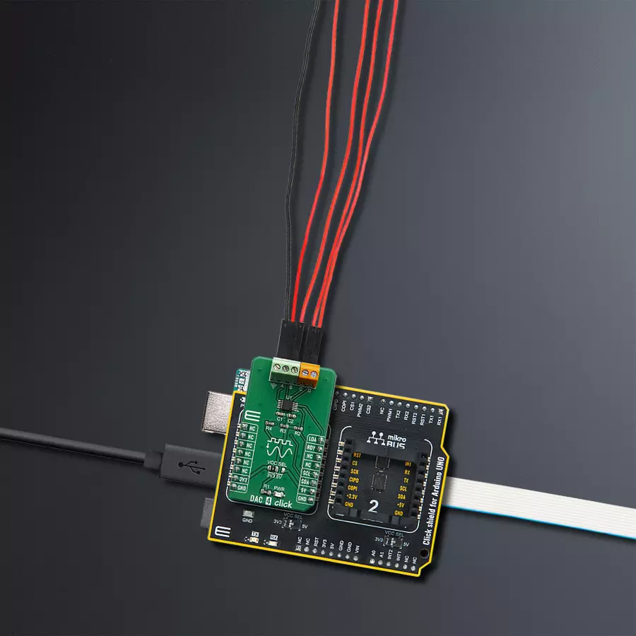
Click Shield for Arduino UNO has two proprietary mikroBUS™ sockets, allowing all the Click board™ devices to be interfaced with the Arduino UNO board without effort. The Arduino Uno, a microcontroller board based on the ATmega328P, provides an affordable and flexible way for users to try out new concepts and build prototypes with the ATmega328P microcontroller from various combinations of performance, power consumption, and features. The Arduino Uno has 14 digital input/output pins (of which six can be used as PWM outputs), six analog inputs, a 16 MHz ceramic resonator (CSTCE16M0V53-R0), a USB connection, a power jack, an ICSP header, and reset button. Most of the ATmega328P microcontroller pins are brought to the IO pins on the left and right edge of the board, which are then connected to two existing mikroBUS™ sockets. This Click Shield also has several switches that perform functions such as selecting the logic levels of analog signals on mikroBUS™ sockets and selecting logic voltage levels of the mikroBUS™ sockets themselves. Besides, the user is offered the possibility of using any Click board™ with the help of existing bidirectional level-shifting voltage translators, regardless of whether the Click board™ operates at a 3.3V or 5V logic voltage level. Once you connect the Arduino UNO board with our Click Shield for Arduino UNO, you can access hundreds of Click boards™, working with 3.3V or 5V logic voltage levels.

Used MCU Pins
mikroBUS™ mapper
Take a closer look
Click board™ Schematic

Step by step
Project assembly

Start by selecting your development board and Click board™. Begin with the Arduino UNO Rev3 as your development board.


Track your results in real time
Application Output
1. Application Output - In Debug mode, the 'Application Output' window enables real-time data monitoring, offering direct insight into execution results. Ensure proper data display by configuring the environment correctly using the provided tutorial.

2. UART Terminal - Use the UART Terminal to monitor data transmission via a USB to UART converter, allowing direct communication between the Click board™ and your development system. Configure the baud rate and other serial settings according to your project's requirements to ensure proper functionality. For step-by-step setup instructions, refer to the provided tutorial.

3. Plot Output - The Plot feature offers a powerful way to visualize real-time sensor data, enabling trend analysis, debugging, and comparison of multiple data points. To set it up correctly, follow the provided tutorial, which includes a step-by-step example of using the Plot feature to display Click board™ readings. To use the Plot feature in your code, use the function: plot(*insert_graph_name*, variable_name);. This is a general format, and it is up to the user to replace 'insert_graph_name' with the actual graph name and 'variable_name' with the parameter to be displayed.

Software Support
Library Description
This library contains API for DAC 4 Click driver.
Key functions:
dac4_voltage_reference_set- Setting channel voltage reference valuesdac4_gain_set- Writing channel gain valuesdac4_data_report- Reading channel data and forming reports
Open Source
Code example
The complete application code and a ready-to-use project are available through the NECTO Studio Package Manager for direct installation in the NECTO Studio. The application code can also be found on the MIKROE GitHub account.
/*!
 * \file
 * \brief Dac4 Click example
 *
 * # Description
 * This application enables usage of digital to analog converter.
 *
 * The demo application is composed of two sections :
 *
 * ## Application Init
 * Initializes I2C driver, executes general call reset and wake up commands.
 *
 * ## Application Task
 * Changes the output voltage of channels every 3 seconds, and displays
 * the channels status on the USB UART.
 *
 * \author MikroE Team
 *
 */
// ------------------------------------------------------------------- INCLUDES

#include "board.h"
#include "log.h"
#include "dac4.h"

// ------------------------------------------------------------------ VARIABLES

static dac4_t dac4;
static log_t logger;

// ------------------------------------------------------- ADDITIONAL FUNCTIONS

void dac4_log_report ( uint8_t channel_no )
{
    dac4_channel_setting_t dac4_channel_buffer[ 8 ];

    dac4_data_report ( &dac4, dac4_channel_buffer );
    channel_no *= 2;

    log_printf( &logger, "--- Power ON bit: " );
    switch ( dac4_channel_buffer[ channel_no ].por_bit )
    {
        case 0:
        {
            log_printf( &logger,"Power OFF\r\n" );
            break;
        }
        case 1:
        {
            log_printf( &logger, "Power ON\r\n" );
            break;
        }
        default :
        {
            break;
        }
    }

    log_printf( &logger, "--- V reference    : " );
    switch ( dac4_channel_buffer[ channel_no ].voltage_reference )
    {
        case DAC4_VREF_EXTERNAL:
        {
            log_printf( &logger, "External\r\n" );
            break;
        }
        case DAC4_VREF_INTERNAL:
        {
            log_printf( &logger, "Internal\r\n" );
            break;
        }
        default :
        {
            break;
        }
    }

    log_printf( &logger, "--- Power mode     : " );
    switch ( dac4_channel_buffer[ channel_no ].power_mode )
    {
        case DAC4_MODE_NORMAL:
        {
            log_printf( &logger, "Normal\r\n" );
            break;
        }
        case DAC4_MODE_1kOhm:
        {
            log_printf( &logger, "1 kOhm\r\n" );
            break;
        }
        case DAC4_MODE_100kOhm:
        {
            log_printf( &logger, "100 kOhm\r\n" );
            break;
        }
        case DAC4_MODE_500kOhm:
        {
            log_printf( &logger, "500 kOhm\r\n" );
            break;
        }
        default :
        {
            break;
        }
    }

    log_printf( &logger, "--- Gain value     : " );
    switch ( dac4_channel_buffer[ channel_no ].gain_value )
    {
        case DAC4_MODE_NORMAL:
        {
            log_printf( &logger, "1x Gain\r\n" );
            break;
        }
        case DAC4_MODE_1kOhm:
        {
            log_printf( &logger, "2x Gain\r\n" );
            break;
        }
        default :
        {
            break;
        }
    }

    log_printf( &logger, "--- DAC input data : %d  [0-4095]\r\n", dac4_channel_buffer[ channel_no ].dac_input_data );
    log_printf( &logger, "-------------------------------------\r\n" );
}

void dac4_set_output ( uint8_t channel_set )
{
    dac4_channel_setting_t dac4_channel_x;
    static uint16_t aux_dac_input_data = 0;

    dac4_channel_x.channel_select = channel_set;
    dac4_channel_x.udac_bit = DAC4_UPDATE;
    dac4_channel_x.voltage_reference = DAC4_VREF_EXTERNAL;
    dac4_channel_x.power_mode = DAC4_MODE_NORMAL;
    dac4_channel_x.gain_value = DAC4_GAIN_x1;
    dac4_channel_x.dac_input_data = aux_dac_input_data;

    if ( 0 != dac4_single_write( &dac4, &dac4_channel_x ) )
    {
        log_printf( &logger, "--- Fatal ERROR !!! \r\n" );
    }
    else
    {
        log_printf( &logger, "------------------------------------- \r\n" );
        log_printf( &logger, "--- Output setup done \r\n" );
        log_printf( &logger, "------------------------------------- \r\n" );
        aux_dac_input_data += 500;
        if ( aux_dac_input_data > 4095 )
        {
            aux_dac_input_data = 0;
        }
    }
}

void dac4_channel_report ( )
{
    log_printf( &logger, "\r\n -----> Channel A \r\n" );
    dac4_set_output( DAC4_CHANNEL_A );
    dac4_log_report( 0 );
    Delay_ms ( 1000 );
    Delay_ms ( 1000 );
    Delay_ms ( 1000 );

    log_printf( &logger, "\r\n -----> Channel B \r\n" );
    dac4_set_output( DAC4_CHANNEL_B );
    dac4_log_report( 1 );
    Delay_ms ( 1000 );
    Delay_ms ( 1000 );
    Delay_ms ( 1000 );

    log_printf( &logger, "\r\n -----> Channel C \r\n" );
    dac4_set_output( DAC4_CHANNEL_C );
    dac4_log_report( 2 );
    Delay_ms ( 1000 );
    Delay_ms ( 1000 );
    Delay_ms ( 1000 );

    log_printf( &logger, "\r\n -----> Channel D \r\n" );
    dac4_set_output( DAC4_CHANNEL_D );
    dac4_log_report( 3 );
    Delay_ms ( 1000 );
    Delay_ms ( 1000 );
    Delay_ms ( 1000 );
}

// ------------------------------------------------------ APPLICATION FUNCTIONS

void application_init ( void )
{
    log_cfg_t log_cfg;
    dac4_cfg_t cfg;

    /**
     * Logger initialization.
     * Default baud rate: 115200
     * Default log level: LOG_LEVEL_DEBUG
     * @note If USB_UART_RX and USB_UART_TX
     * are defined as HAL_PIN_NC, you will
     * need to define them manually for log to work.
     * See @b LOG_MAP_USB_UART macro definition for detailed explanation.
     */
    LOG_MAP_USB_UART( log_cfg );
    log_init( &logger, &log_cfg );
    log_info( &logger, "---- Application Init ----" );

    //  Click initialization.

    dac4_cfg_setup( &cfg );
    DAC4_MAP_MIKROBUS( cfg, MIKROBUS_1 );
    dac4_init( &dac4, &cfg );
    log_info( &logger, "---- Application ----" );

    Delay_ms ( 500 );
    dac4_general_call_reset( &dac4 );
    Delay_ms ( 500 );
    dac4_general_call_wake_up( &dac4 );
    Delay_ms ( 500 );

    log_printf( &logger, "--- App init done \r\n \r\n" );
}

void application_task ( void )
{
    dac4_channel_report( );
}

int main ( void )
{
    /* Do not remove this line or clock might not be set correctly. */
    #ifdef PREINIT_SUPPORTED
    preinit();
    #endif

    application_init( );

    for ( ; ; )
    {
        application_task( );
    }

    return 0;
}

// ------------------------------------------------------------------------ END
Additional Support
Resources
Category:DAC