Ensure a stable and reliable output voltage with minimal dropout with TPS7A83A and ATmega328P
Unlocking efficiency in voltage control
Published Feb 14, 2024
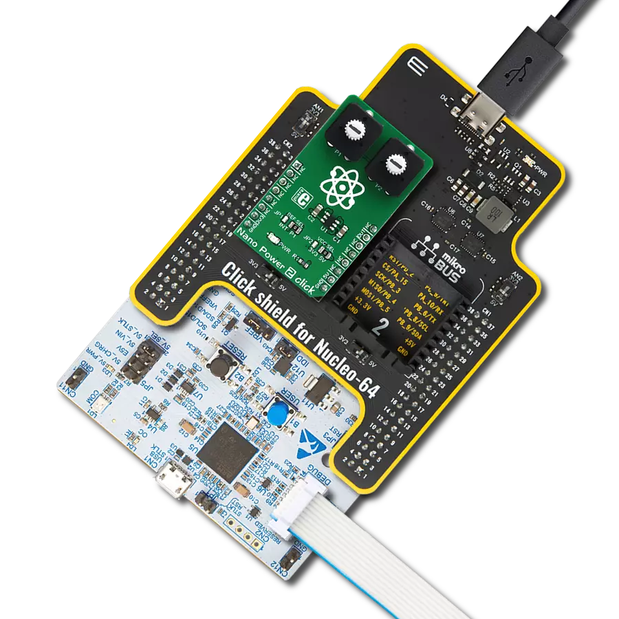
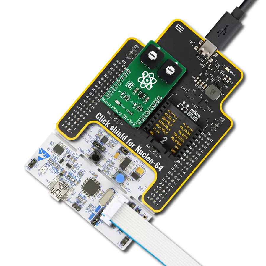
Click board™
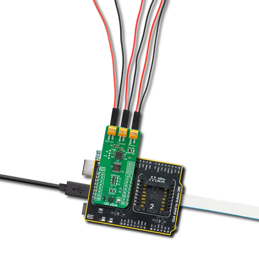
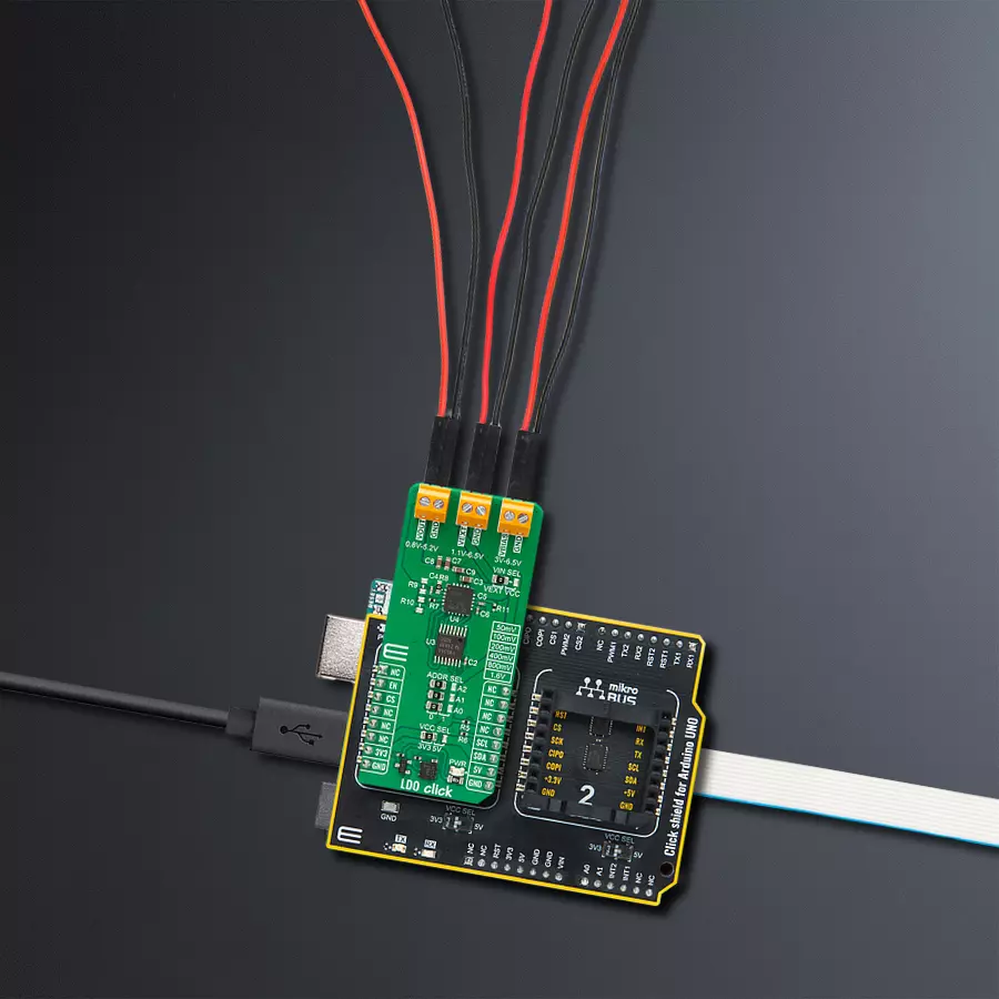
LDO Click
Dev. board
Arduino UNO Rev3
Compiler
NECTO Studio
MCU
ATmega328P
Witness voltage precision and dropout perfection with LDO regulators that set the standard for accurate and efficient voltage control
A
A
Hardware Overview
How does it work?
LDO Click is based on the TPS7A83A, a high-current (2A), low-noise, high-accuracy, and low-dropout linear voltage regulator from Texas Instruments. The TPS7A83A has several features that make it useful in various applications, like high accuracy, high-PSR output, and fast transient response for voltage regulation part, as well as certain internal protections like thermal shutdown and foldback current limit. All these features make this Click board™ a robust solution for many challenging problems in generating a clean, accurate power supply. The TPS7A8300A can be easily enabled using the EN pin of the mikroBUS™ socket, offering a switch operation to turn ON/OFF the TPS7A8300A. It has a pin-programmable output voltage from 0.8V-3.95V with a 50mV resolution, or it can be adjustable from 0.8V-5.2V using an external resistor divider (R9 and R10). The
pin-programmable output voltage is possible thanks to the TCA9534A, an I2C-configurable I/O expander also from Texas Instruments, which, by setting the appropriate voltage setting pins on the TPS7A83A, which are connected to an internal feedback network, programs the regulated output voltage. The TCA9534A expander can also choose the least significant bit (LSB) of its I2C slave address by positioning SMD jumpers labeled ADDR SEL to an appropriate position marked as 0 and 1. The adjustable output voltage is achieved through voltage divider resistors whose corresponding values can be found in the datasheet table. One of the power terminals on the board is the VBIAS terminal, which minimizes the internal charge-pump noise when the internal voltage is clamped, thereby reducing the overall output noise floor. This rail enables the use of
low-input voltage, low-output (LILO) voltage conditions (VEXT=1.2V, VOUT =1V) to reduce the power dissipation of the TPS7A8300A. Using a VBIAS voltage improves DC and AC performance for VEXT≤2.2V. This Click board™ can operate with either 3.3V or 5V logic voltage levels selected via the VCC SEL jumper. This way, it is allowed for both 3.3V and 5V capable MCUs to use the communication lines properly. Additionally, there is a possibility for the TPS7A83A power supply selection via jumper labeled as VIN SEL to supply the TPS7A83A from an external power supply terminal in the range from 1.1V to 6.5V or with selected mikroBUS™ power rail. However, the Click board™ comes equipped with a library containing easy-to-use functions and an example code that can be used as a reference for further development.

Features overview
Development board
Arduino UNO is a versatile microcontroller board built around the ATmega328P chip. It offers extensive connectivity options for various projects, featuring 14 digital input/output pins, six of which are PWM-capable, along with six analog inputs. Its core components include a 16MHz ceramic resonator, a USB connection, a power jack, an
ICSP header, and a reset button, providing everything necessary to power and program the board. The Uno is ready to go, whether connected to a computer via USB or powered by an AC-to-DC adapter or battery. As the first USB Arduino board, it serves as the benchmark for the Arduino platform, with "Uno" symbolizing its status as the
first in a series. This name choice, meaning "one" in Italian, commemorates the launch of Arduino Software (IDE) 1.0. Initially introduced alongside version 1.0 of the Arduino Software (IDE), the Uno has since become the foundational model for subsequent Arduino releases, embodying the platform's evolution.

Microcontroller Overview
MCU Card / MCU

Architecture
AVR
MCU Memory (KB)
32
Silicon Vendor
Microchip
Pin count
28
RAM (Bytes)
2048
You complete me!
Accessories
Click Shield for Arduino UNO has two proprietary mikroBUS™ sockets, allowing all the Click board™ devices to be interfaced with the Arduino UNO board without effort. The Arduino Uno, a microcontroller board based on the ATmega328P, provides an affordable and flexible way for users to try out new concepts and build prototypes with the ATmega328P microcontroller from various combinations of performance, power consumption, and features. The Arduino Uno has 14 digital input/output pins (of which six can be used as PWM outputs), six analog inputs, a 16 MHz ceramic resonator (CSTCE16M0V53-R0), a USB connection, a power jack, an ICSP header, and reset button. Most of the ATmega328P microcontroller pins are brought to the IO pins on the left and right edge of the board, which are then connected to two existing mikroBUS™ sockets. This Click Shield also has several switches that perform functions such as selecting the logic levels of analog signals on mikroBUS™ sockets and selecting logic voltage levels of the mikroBUS™ sockets themselves. Besides, the user is offered the possibility of using any Click board™ with the help of existing bidirectional level-shifting voltage translators, regardless of whether the Click board™ operates at a 3.3V or 5V logic voltage level. Once you connect the Arduino UNO board with our Click Shield for Arduino UNO, you can access hundreds of Click boards™, working with 3.3V or 5V logic voltage levels.

Used MCU Pins
mikroBUS™ mapper
Take a closer look
Click board™ Schematic

Step by step
Project assembly

Start by selecting your development board and Click board™. Begin with the Arduino UNO Rev3 as your development board.


Software Support
Library Description
This library contains API for LDO Click driver.
Key functions:
ldo_enable_device- This function enables the device by setting the EN pin to HIGH logic stateldo_disable_device- This function disables the device by setting the EN pin to LOW logic stateldo_set_vout- This function sets the voltage output.
Open Source
Code example
The complete application code and a ready-to-use project are available through the NECTO Studio Package Manager for direct installation in the NECTO Studio. The application code can also be found on the MIKROE GitHub account.
/*!
 * @file main.c
 * @brief LDO Click example
 *
 * # Description
 * This example demonstrates the use of LDO Click by changing the output voltage.
 *
 * The demo application is composed of two sections :
 *
 * ## Application Init
 * Initializes the driver and performs the device default configuration.
 *
 * ## Application Task
 * Changes the output voltage every 3 seconds and displays on the USB UART
 * the currently set voltage output value.
 *
 * @note
 * In order to have up to 3950mV at VOUT you will need to move the VIN SEL on-board jumper
 * to the VEXT position and provide at least 3950mV voltage input at the VEXT terminal.
 * Otherwise, the maximum level of VOUT will be limited to 3.3V system voltage.
 *
 * @author Stefan Filipovic
 *
 */

#include "board.h"
#include "log.h"
#include "ldo.h"

static ldo_t ldo;
static log_t logger;

void application_init ( void )
{
    log_cfg_t log_cfg;  /**< Logger config object. */
    ldo_cfg_t ldo_cfg;  /**< Click config object. */

    /**
     * Logger initialization.
     * Default baud rate: 115200
     * Default log level: LOG_LEVEL_DEBUG
     * @note If USB_UART_RX and USB_UART_TX
     * are defined as HAL_PIN_NC, you will
     * need to define them manually for log to work.
     * See @b LOG_MAP_USB_UART macro definition for detailed explanation.
     */
    LOG_MAP_USB_UART( log_cfg );
    log_init( &logger, &log_cfg );
    log_info( &logger, " Application Init " );

    // Click initialization.
    ldo_cfg_setup( &ldo_cfg );
    LDO_MAP_MIKROBUS( ldo_cfg, MIKROBUS_1 );
    if ( I2C_MASTER_ERROR == ldo_init( &ldo, &ldo_cfg ) )
    {
        log_error( &logger, " Communication init." );
        for ( ; ; );
    }

    if ( LDO_ERROR == ldo_default_cfg ( &ldo ) )
    {
        log_error( &logger, " Default configuration." );
        for ( ; ; );
    }

    log_info( &logger, " Application Task " );
}

void application_task ( void )
{
    static uint16_t vout = LDO_VOUT_MIN;
    if ( LDO_OK == ldo_set_vout ( &ldo, vout ) )
    {
        log_printf ( &logger, " VOUT: %u mV\r\n\n", vout );
    }
    vout += LDO_VOUT_STEP;
    if ( vout > LDO_VOUT_MAX )
    {
        vout = LDO_VOUT_MIN;
    }
    Delay_ms ( 1000 );
    Delay_ms ( 1000 );
    Delay_ms ( 1000 );
}

int main ( void )
{
    /* Do not remove this line or clock might not be set correctly. */
    #ifdef PREINIT_SUPPORTED
    preinit();
    #endif

    application_init( );

    for ( ; ; )
    {
        application_task( );
    }

    return 0;
}

// ------------------------------------------------------------------------ END
Additional Support
Resources
Category:Linear