Achieve best-in-class non-volatile memory with long data retention using MR25H256 and PIC24FV16KA302
Dive into the world of MRAM

Published Sep 13, 2023
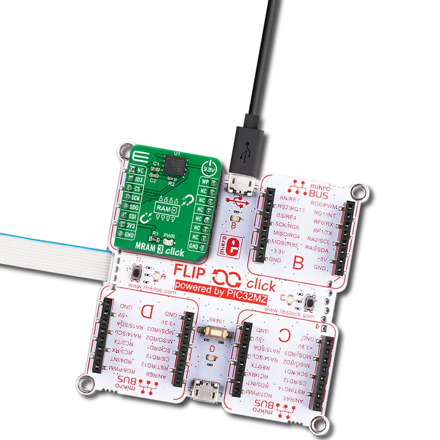
Click board™
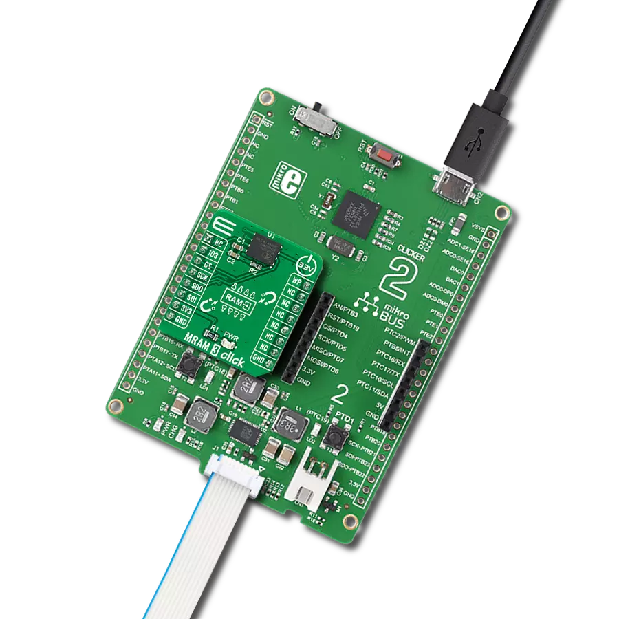
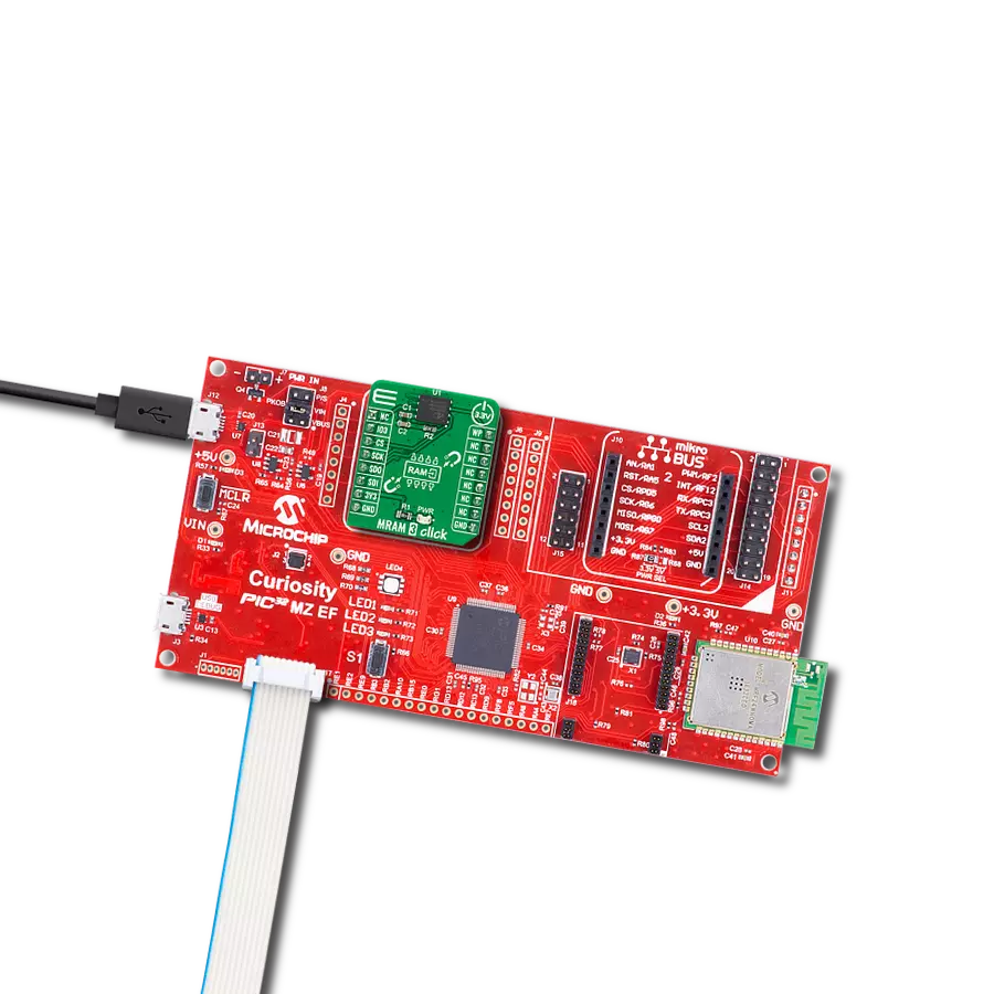
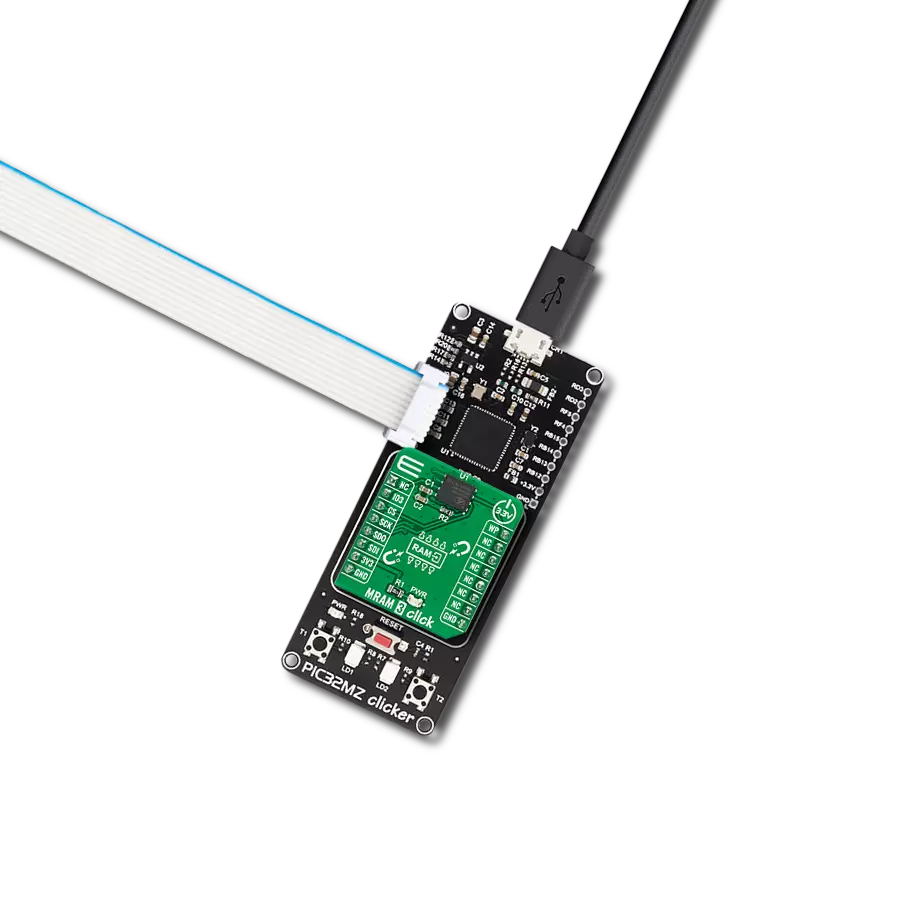
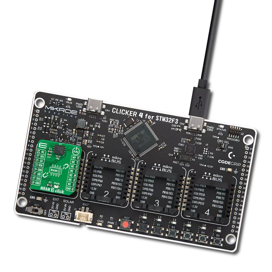
MRAM Click
Dev. board
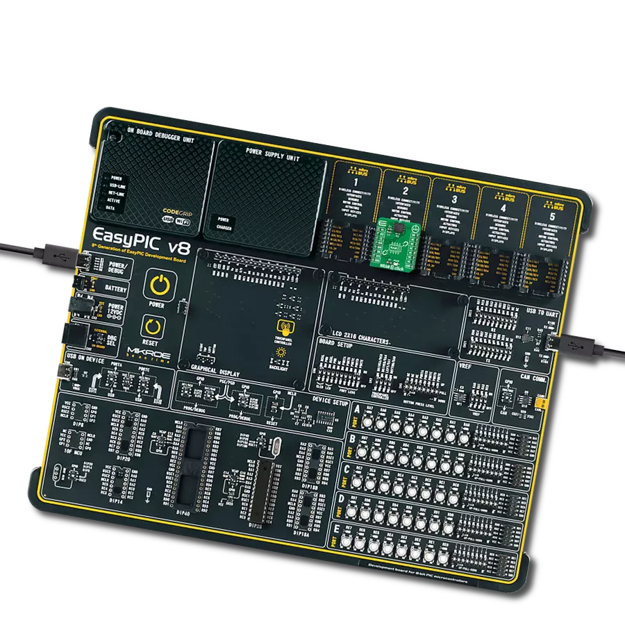
EasyPIC v8 for PIC24/dsPIC33
Compiler
NECTO Studio
MCU
PIC24FV16KA302
Trust MRAM as your data's guardian. Our solution offers persistent memory with rapid read and write capabilities, ensuring data integrity and fast access for applications where reliability is paramount.
A
A
Hardware Overview
How does it work?
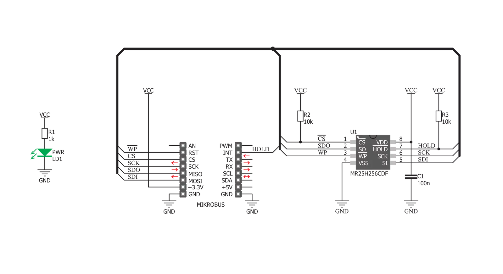
MRAM Click is based on the MR25H256, a 256 kilobits serial SPI MRAM memory module from Everspin company. This module contains 262,144 bits of memory that can be randomly accessed. The pinout of the used memory module is the same as most commonly used EEPROM modules so that it can directly replace it. The usual SPI lines - SO, SI, SCK and #CS pins from the MR25H256 IC are routed to the mikroBUS™ SPI port (MISO, MOSI, SCK and CS pins). Besides the SPI serial bus, there are two more pins routed to the mikroBUS™. The #HOLD pin of the MR25H256 IC is routed to the INT pin of the mikroBUS™ and it is used to hold the data transfer. When this pin is pulled to a LOW logic level, all data transfer operations are suspended. However, this function is enabled only when the device is already addressed with the CS pin pulled to a LOW level.
This allows to pause the data transfer and resume it later without the need to first address it via the CS pin, reducing the output latency that way. While the data transfer is paused, the SO pin will switch to a high impedance mode (HIGH Z) and will remain inactive. The SCK pulses are completely ignored. The #HOLD pin of the MR25H256 IC is pulled to a HIGH logic level by an onboard pull-up resistor. The #WP pin of the MR25H256 IC is routed to the INT pin of the mikroBUS™ and it is used to prevent writes to the status register, acting as a hardware write protect pin. It is routed to the RST pin of the mikroBUS™. The logical organization of the moduke, such as read and write commands and the status register of the MR25H256 IC are the same as with most commonly used EEPROM modules, such as the one used in EEPROM 4 Click. That allows this
memory module, as well as MRAM click to replace the existing EEPROM module with not too much additional work. The provided libraries offer all the functions needed to work with the MRAM click. Their usage is demonstrated in the included example application which can be used as a reference for further development. The device should wait for the system voltage to become stable before the writing is attempted. This Click board™ can be operated only with a 3.3V logic voltage level. The board must perform appropriate logic voltage level conversion before using MCUs with different logic levels. Also, it comes equipped with a library containing functions and an example code that can be used as a reference for further development.


Features overview
Development board
EasyPIC v8 for PIC24/dsPIC33 is a development board specially designed for the needs of rapid development of embedded applications. It supports a wide range of 16-bit PIC24/dsPIC33 microcontrollers from Microchip and has a broad set of unique functions, such as the first-ever embedded debugger/programmer. The development board is well organized and designed so that the end-user has all the necessary elements, such as switches, buttons, indicators, connectors, and others, in one place. Thanks to innovative manufacturing technology, EasyPIC v8 for PIC24/dsPIC33 provides a fluid and immersive working experience, allowing access anywhere and under any circumstances. Each part of the EasyPIC
v8 for PIC24/dsPIC33 development board contains the components necessary for the most efficient operation of the same board. In addition to the advanced integrated CODEGRIP programmer/debugger module, which offers many valuable programming/debugging options and seamless integration with the Mikroe software environment, the board also includes a clean and regulated power supply module for the development board. It can use a wide range of external power sources, including a battery, an external 12V power supply, and a power source via the USB Type-C (USB-C) connector. Communication options such as USB HOST/DEVICE, USB-UART, CAN, and LIN are also
included, including the well-established mikroBUS™ standard, two display options (graphical and character-based LCD), and several different DIP sockets. These sockets cover a wide range of 16-bit PIC24/dsPIC33 MCUs, from the smallest PIC24/dsPIC33 MCUs with only 14 up to 28 pins. EasyPIC v8 for PIC24/dsPIC33 is an integral part of the Mikroe ecosystem for rapid development. Natively supported by Mikroe software tools, it covers many aspects of prototyping and development thanks to a considerable number of different Click boards™ (over a thousand boards), the number of which is growing every day.

Microcontroller Overview
MCU Card / MCU
Architecture
dsPIC
MCU Memory (KB)
16
Silicon Vendor
Microchip
Pin count
28
RAM (Bytes)
2048
Used MCU Pins
mikroBUS™ mapper
Take a closer look
Click board™ Schematic
Step by step
Project assembly

Start by selecting your development board and Click board™. Begin with the EasyPIC v8 for PIC24/dsPIC33 as your development board.


Software Support
Library Description
This library contains API for MRAM Click driver.
Key functions:
mram_write_data_bytes- Function writes n bytes of data from the buffermram_read_data_bytes- Function reads n bytes of data and saves it in buffermram_enable_write_protect- Function enables or disables write protect.
Open Source
Code example
The complete application code and a ready-to-use project are available through the NECTO Studio Package Manager for direct installation in the NECTO Studio. The application code can also be found on the MIKROE GitHub account.
/*!
 * \file
 * \brief MRAM Click example
 *
 * # Description
 * This example writes and reads from the Mram Click and displays it on the terminal.
 *
 * The demo application is composed of two sections :
 *
 * ## Application Init
 * Initializes Click driver.
 *
 * ## Application Task
 * Writes 10 bytes of buffer data in memory with start address 0x0001. Then reads
 * 10 bytes from memory with start address 0x0001 and shows result on USB UART.
 *
 *
 * \author MikroE Team
 *
 */
// ------------------------------------------------------------------- INCLUDES

#include "board.h"
#include "log.h"
#include "mram.h"

// ------------------------------------------------------------------ VARIABLES

static mram_t mram;
static log_t logger;

// ------------------------------------------------------ APPLICATION FUNCTIONS

void application_init ( void )
{
    log_cfg_t log_cfg;
    mram_cfg_t cfg;

    /**
     * Logger initialization.
     * Default baud rate: 115200
     * Default log level: LOG_LEVEL_DEBUG
     * @note If USB_UART_RX and USB_UART_TX
     * are defined as HAL_PIN_NC, you will
     * need to define them manually for log to work.
     * See @b LOG_MAP_USB_UART macro definition for detailed explanation.
     */
    LOG_MAP_USB_UART( log_cfg );
    log_init( &logger, &log_cfg );
    log_info( &logger, "---- Application Init ----" );

    //  Click initialization.

    mram_cfg_setup( &cfg );
    MRAM_MAP_MIKROBUS( cfg, MIKROBUS_1 );
    mram_init( &mram, &cfg );
    mram_default_cfg( &mram );

}

void application_task ( void )
{
    uint8_t number_bytes_write;
    uint8_t number_bytes_read;
    uint16_t i;
    uint8_t data_write[ 10 ] = { 1, 2, 3, 4, 5, 6, 7, 8, 9, 10 };
    uint8_t data_read[ 20 ] = { 0 };

    number_bytes_write = 10;
    number_bytes_read = 10;

    log_printf( &logger, " Data written!\r\n" );
    mram_write_data_bytes ( &mram, 0x0001, data_write, number_bytes_write );

    log_printf( &logger, " Read data:\r\n" );
    mram_read_data_bytes ( &mram, 0x0001, data_read, number_bytes_read );

    for ( i = 0; i < number_bytes_read; i++ )
    {
        log_printf( &logger, "%d ", ( uint16_t )data_read[ i ] );
    }

    log_printf( &logger, "\n" );

    Delay_ms ( 1000 );
    Delay_ms ( 1000 );
    Delay_ms ( 1000 );
}

int main ( void )
{
    /* Do not remove this line or clock might not be set correctly. */
    #ifdef PREINIT_SUPPORTED
    preinit();
    #endif

    application_init( );

    for ( ; ; )
    {
        application_task( );
    }

    return 0;
}

// ------------------------------------------------------------------------ END
Additional Support
Resources
Category:MRAM