Convert analog to digital signals with AD7091R and STM32F746ZG with additional electrical isolation between them
Isolate and digitize with precision

Published Sep 17, 2024
Click board™
ISO ADC 2 Click
Dev. board
Nucleo 144 with STM32F746ZG MCU
Compiler
NECTO Studio
MCU
STM32F746ZG
Unleash the power of isolation with our cutting-edge A/D converter!
A
A
Hardware Overview
How does it work?
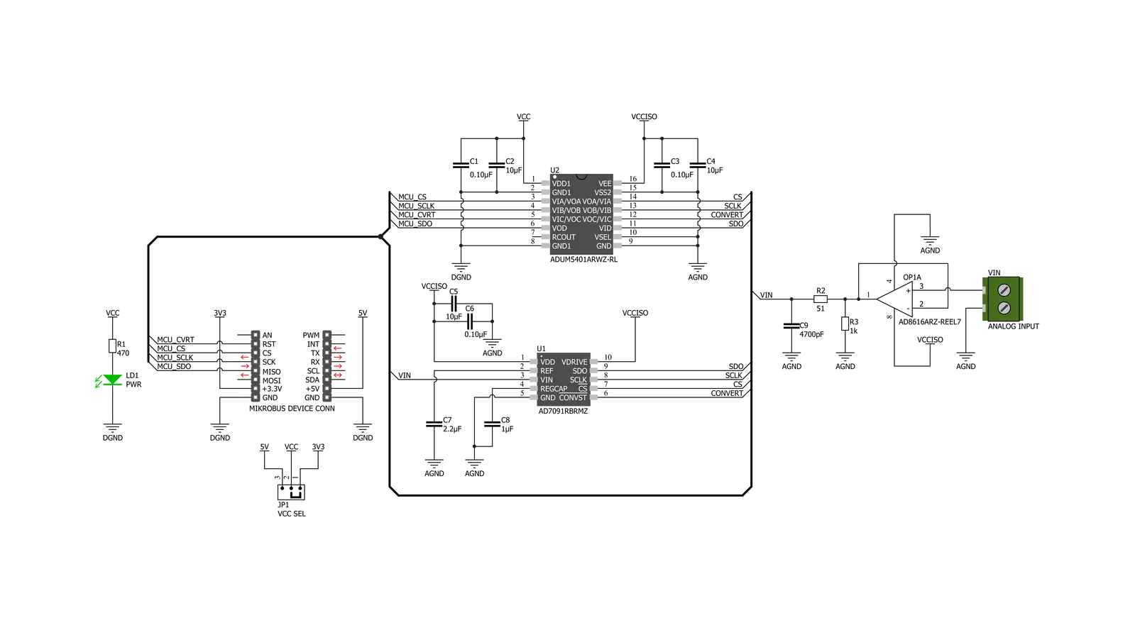
ISO ADC 2 Click is based on the AD7091R, a 12-bit successive-approximation analog-to-digital converter (ADC) with an isolated DC-DC converter from Analog Devices. This Click board™ allows single-supply operation and consists of active Analog Devices components: AD8616, a level shifting circuit; AD7091R, an ADC stage; and ADuM5401, an output isolation stage. The AD8616 is chosen for this application because of its low offset voltage, low bias current, and low noise. The output of the OpAmp is 0.1V to 2.4V, which matches the input range of the ADC (0V to 2.5V) with a 100mV safety margin to maintain linearity. A single-pole RC filter (R2/C9) follows the OpAmp output stage to reduce the out-of-band noise. The next part of the circuit is the AD7091R, ADC chosen because of its
ultralow power, which is significantly lower than any competitive A/D converter. It features a power-down option, implemented across the serial interface to save power between conversions, described in the Modes of Operation section in the datasheet. After a successful conversion, the ADC sends the data to the MCU through galvanic isolation provided by the ADuM5401 quad-channel digital isolator with an integrated DC-DC converter. The isolator has a secondary side controller architecture with isolated pulse-width modulation (PWM) feedback, and it works on the principle common to most switching power supplies. The ISO ADC 2 Click communicates with MCU using the 3-wire SPI serial interface that operates at clock rates up to 50MHz used for accessing data from the result register
and controlling the device's modes of operation. The CONVST signal of the AD7091R routed to the RST pin on the mikroBUS™ is used to initiate the conversion process, data acquisition, and select the operation mode. This ADC requires the user to initiate a software reset upon Power-Up, and it should be noted that failure to apply the correct software reset command may result in a device malfunction. This Click board™ can operate with either 3.3V or 5V logic voltage levels selected via the VCC SEL jumper. This way, both 3.3V and 5V capable MCUs can use the communication lines properly. However, the Click board™ comes equipped with a library containing easy-to-use functions and an example code that can be used, as a reference, for further development.


Features overview
Development board
Nucleo-144 with STM32F746ZG MCU board offers an accessible and adaptable avenue for users to explore new ideas and construct prototypes. It allows users to tailor their experience by selecting from a range of performance and power consumption features offered by the STM32 microcontroller. With compatible boards, the
internal or external SMPS dramatically decreases power usage in Run mode. Including the ST Zio connector, expanding ARDUINO Uno V3 connectivity, and ST morpho headers facilitate easy expansion of the Nucleo open development platform. The integrated ST-LINK debugger/programmer enhances convenience by
eliminating the need for a separate probe. Moreover, the board is accompanied by comprehensive free software libraries and examples within the STM32Cube MCU Package, further enhancing its utility and value.

Microcontroller Overview
MCU Card / MCU

Architecture
ARM Cortex-M7
MCU Memory (KB)
1024
Silicon Vendor
STMicroelectronics
Pin count
144
RAM (Bytes)
327680
You complete me!
Accessories
Click Shield for Nucleo-144 comes equipped with four mikroBUS™ sockets, with one in the form of a Shuttle connector, allowing all the Click board™ devices to be interfaced with the STM32 Nucleo-144 board with no effort. This way, MIKROE allows its users to add any functionality from our ever-growing range of Click boards™, such as WiFi, GSM, GPS, Bluetooth, ZigBee, environmental sensors, LEDs, speech recognition, motor control, movement sensors, and many more. Featuring an ARM Cortex-M microcontroller, 144 pins, and Arduino™ compatibility, the STM32 Nucleo-144 board offers limitless possibilities for prototyping and creating diverse applications. These boards are controlled and powered conveniently through a USB connection to program and efficiently debug the Nucleo-144 board out of the box, with an additional USB cable connected to the USB mini port on the board. Simplify your project development with the integrated ST-Link debugger and unleash creativity using the extensive I/O options and expansion capabilities. This Click Shield also has several switches that perform functions such as selecting the logic levels of analog signals on mikroBUS™ sockets and selecting logic voltage levels of the mikroBUS™ sockets themselves. Besides, the user is offered the possibility of using any Click board™ with the help of existing bidirectional level-shifting voltage translators, regardless of whether the Click board™ operates at a 3.3V or 5V logic voltage level. Once you connect the STM32 Nucleo-144 board with our Click Shield for Nucleo-144, you can access hundreds of Click boards™, working with 3.3V or 5V logic voltage levels.

Used MCU Pins
mikroBUS™ mapper
Take a closer look
Click board™ Schematic
Step by step
Project assembly
Start by selecting your development board and Click board™. Begin with the Nucleo 144 with STM32F746ZG MCU as your development board.


Track your results in real time
Application Output
1. Application Output - In Debug mode, the 'Application Output' window enables real-time data monitoring, offering direct insight into execution results. Ensure proper data display by configuring the environment correctly using the provided tutorial.

2. UART Terminal - Use the UART Terminal to monitor data transmission via a USB to UART converter, allowing direct communication between the Click board™ and your development system. Configure the baud rate and other serial settings according to your project's requirements to ensure proper functionality. For step-by-step setup instructions, refer to the provided tutorial.

3. Plot Output - The Plot feature offers a powerful way to visualize real-time sensor data, enabling trend analysis, debugging, and comparison of multiple data points. To set it up correctly, follow the provided tutorial, which includes a step-by-step example of using the Plot feature to display Click board™ readings. To use the Plot feature in your code, use the function: plot(*insert_graph_name*, variable_name);. This is a general format, and it is up to the user to replace 'insert_graph_name' with the actual graph name and 'variable_name' with the parameter to be displayed.

Software Support
Library Description
This library contains API for ISO ADC 2 Click driver.
Key functions:
uint16_t isoadc2_read_adc ( void )Function for reading 12bit ADC datauint16_t isoadc2_get_mv ( uint16_t adc_data )Function for converting ADC to mV data
Open Source
Code example
The complete application code and a ready-to-use project are available through the NECTO Studio Package Manager for direct installation in the NECTO Studio. The application code can also be found on the MIKROE GitHub account.
/*!
 * @file main.c
 * @brief IsoAdc2 Click example
 *
 * # Description
 * This is an example that demonstrates the use of the ISO ADC 2 Click board.
 *
 * The demo application is composed of two sections :
 *
 * ## Application Init
 * Initialization of SPI module and additional GPIO pins.
 *
 * ## Application Task
 * Every second reads ADC data and voltage in mV and logs result.
 *
 * @author Stefan Ilic
 *
 */

#include "board.h"
#include "log.h"
#include "isoadc2.h"

static isoadc2_t isoadc2;
static log_t logger;

void application_init ( void ) {
    log_cfg_t log_cfg;  /**< Logger config object. */
    isoadc2_cfg_t isoadc2_cfg;  /**< Click config object. */

    /**
     * Logger initialization.
     * Default baud rate: 115200
     * Default log level: LOG_LEVEL_DEBUG
     * @note If USB_UART_RX and USB_UART_TX
     * are defined as HAL_PIN_NC, you will
     * need to define them manually for log to work.
     * See @b LOG_MAP_USB_UART macro definition for detailed explanation.
     */
    LOG_MAP_USB_UART( log_cfg );
    log_init( &logger, &log_cfg );
    log_info( &logger, " Application Init " );

    // Click initialization.

    isoadc2_cfg_setup( &isoadc2_cfg );
    ISOADC2_MAP_MIKROBUS( isoadc2_cfg, MIKROBUS_1 );
    err_t init_flag  = isoadc2_init( &isoadc2, &isoadc2_cfg );
    if ( SPI_MASTER_ERROR == init_flag ) {
        log_error( &logger, " Application Init Error. " );
        log_info( &logger, " Please, run program again... " );

        for ( ; ; );
    }
    log_info( &logger, " Application Task " );
}

void application_task ( void ) {
    uint16_t rx_data;
    uint16_t mv_data;

    isoadc2_read_adc( &isoadc2, &rx_data );
    Delay_ms( 100 );
    isoadc2_get_mv( &isoadc2, &mv_data );

    log_printf( &logger, " ADC: %d \r\n", rx_data );
    log_printf( &logger, " VIN: %d mV\r\n", mv_data );
    log_printf( &logger, "---------------\r\n" );

    Delay_ms( 1000 );
}

void main ( void ) {
    application_init( );

    for ( ; ; ) {
        application_task( );
    }
}

// ------------------------------------------------------------------------ END


