Simplify the connection of other add-ons to the mikroBUS™ socket with IDC10 header and STM32F030R8
Make compatibility a non-issue!

Published Feb 26, 2024
Click board™
Adapter Click
Dev. board
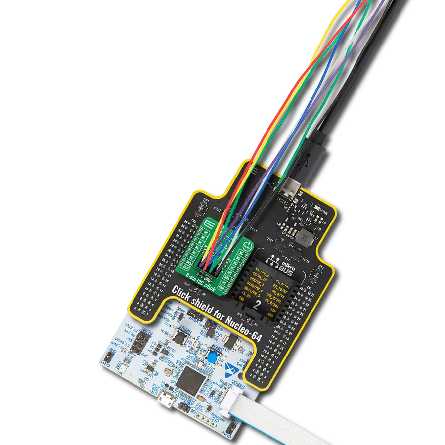
Nucleo-64 with STM32F030R8 MCU
Compiler
NECTO Studio
MCU
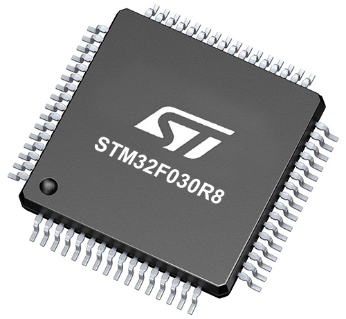
STM32F030R8
Integrate sensors, drivers, and other components into your project setup without hassle
A
A
Hardware Overview
How does it work?
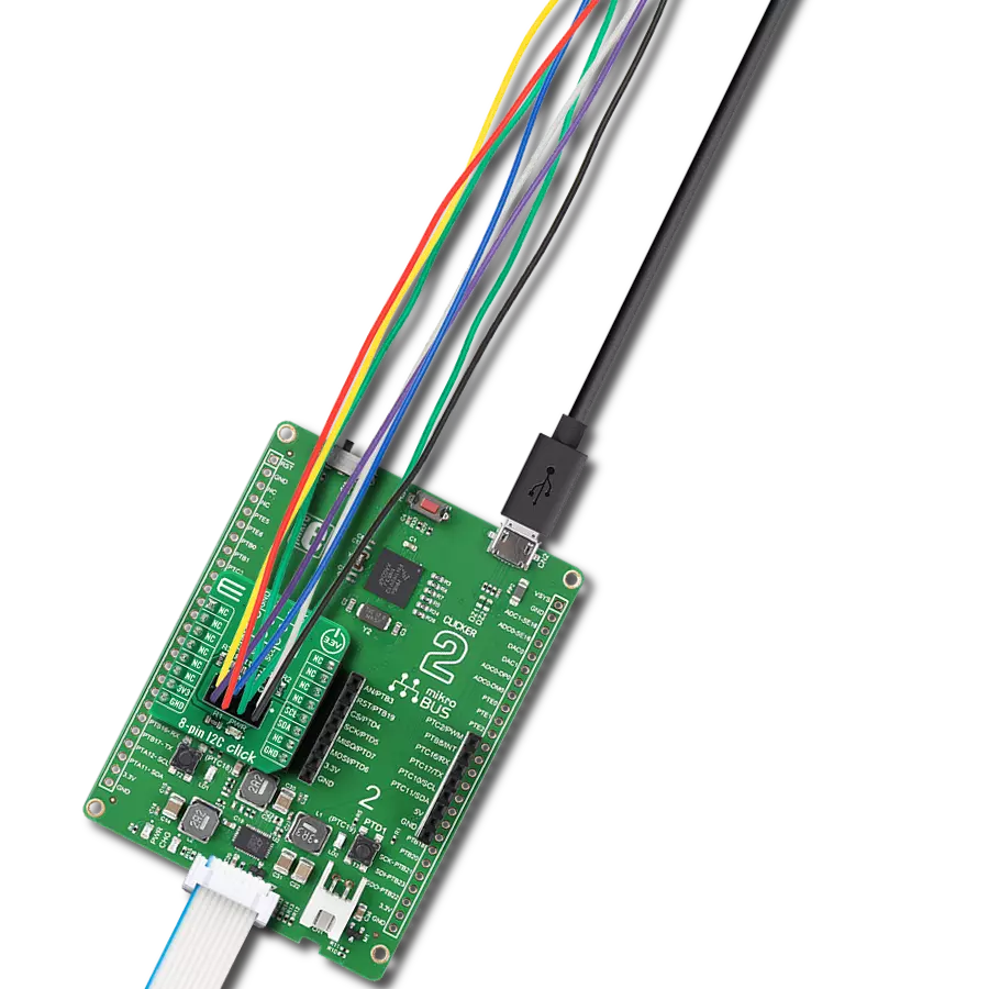
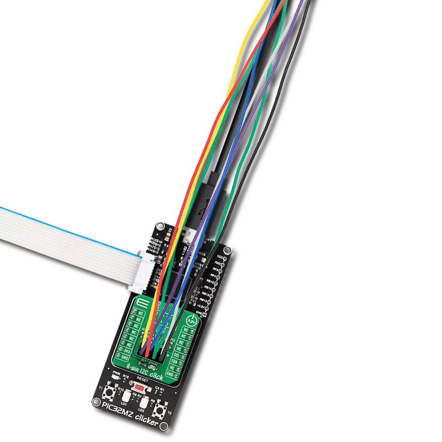
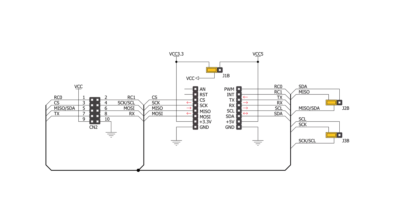
Adapter Click represents an adapter board that simplifies the connection of add-ons with IDC10 headers to the mikroBUS™ socket. One 2x5-position 2.54mm pitch header allows you to add sensors, drivers, and various components in a way that suits your project needs. Each header pin corresponds to a pin on the mikroBUS™ socket (except AN and RST pins). Thanks to these pins, the connection with the Click board™ remains firm and stable, always retaining a perfect connection quality. There are two ways to establish such a connection: male or female IDC10 connectors. Both
are provided with the package. You may solder the male IDC10 header on the top side of the Adapter Click and connect the add-on board directly or via IDC10 flat cable. In some cases, a female header socket is a better choice. Solder it either on the top or the bottom side, depending on which is more convenient in given circumstances. Adapter Click allows using both I2C and SPI interfaces, where each mikroBUS™ line is covered, except, as mentioned before, AN and RST lines. The selection can be made by positioning jumpers labeled as INTERFACE SELECTION in an appropriate
position marked as SPI or I2C. Note that all the jumpers' positions must be on the same side, or the Click board™ may become unresponsive. This Click board™ can operate with both 3.3V and 5V logic voltage levels selected via the PWR SEL jumper. This way, it is allowed for both 3.3V and 5V capable MCUs to use the communication lines properly. Also, this Click board™ comes equipped with a library containing easy-to-use functions and an example code that can be used as a reference for further development.

Features overview
Development board
Nucleo-64 with STM32F030R8 MCU offers a cost-effective and adaptable platform for developers to explore new ideas and prototype their designs. This board harnesses the versatility of the STM32 microcontroller, enabling users to select the optimal balance of performance and power consumption for their projects. It accommodates the STM32 microcontroller in the LQFP64 package and includes essential components such as a user LED, which doubles as an ARDUINO® signal, alongside user and reset push-buttons, and a 32.768kHz crystal oscillator for precise timing operations. Designed with expansion and flexibility in mind, the Nucleo-64 board features an ARDUINO® Uno V3 expansion connector and ST morpho extension pin
headers, granting complete access to the STM32's I/Os for comprehensive project integration. Power supply options are adaptable, supporting ST-LINK USB VBUS or external power sources, ensuring adaptability in various development environments. The board also has an on-board ST-LINK debugger/programmer with USB re-enumeration capability, simplifying the programming and debugging process. Moreover, the board is designed to simplify advanced development with its external SMPS for efficient Vcore logic supply, support for USB Device full speed or USB SNK/UFP full speed, and built-in cryptographic features, enhancing both the power efficiency and security of projects. Additional connectivity is
provided through dedicated connectors for external SMPS experimentation, a USB connector for the ST-LINK, and a MIPI® debug connector, expanding the possibilities for hardware interfacing and experimentation. Developers will find extensive support through comprehensive free software libraries and examples, courtesy of the STM32Cube MCU Package. This, combined with compatibility with a wide array of Integrated Development Environments (IDEs), including IAR Embedded Workbench®, MDK-ARM, and STM32CubeIDE, ensures a smooth and efficient development experience, allowing users to fully leverage the capabilities of the Nucleo-64 board in their projects.

Microcontroller Overview
MCU Card / MCU
Architecture
ARM Cortex-M0
MCU Memory (KB)
64
Silicon Vendor
STMicroelectronics
Pin count
64
RAM (Bytes)
8192
You complete me!
Accessories
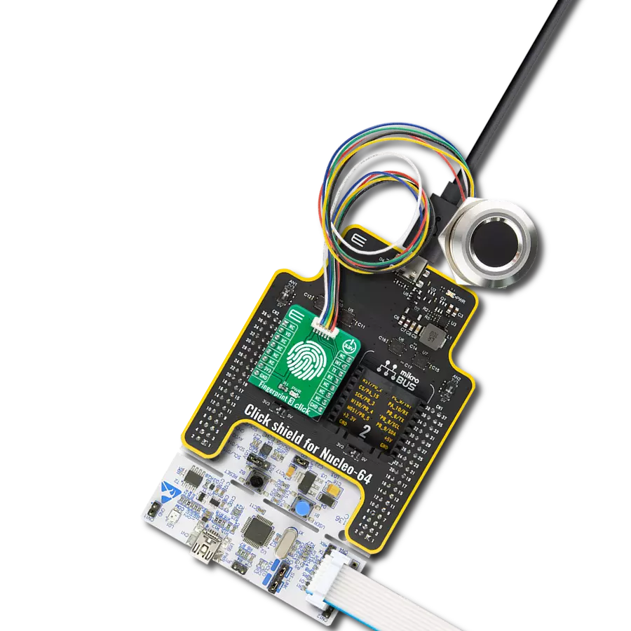
Click Shield for Nucleo-64 comes equipped with two proprietary mikroBUS™ sockets, allowing all the Click board™ devices to be interfaced with the STM32 Nucleo-64 board with no effort. This way, Mikroe allows its users to add any functionality from our ever-growing range of Click boards™, such as WiFi, GSM, GPS, Bluetooth, ZigBee, environmental sensors, LEDs, speech recognition, motor control, movement sensors, and many more. More than 1537 Click boards™, which can be stacked and integrated, are at your disposal. The STM32 Nucleo-64 boards are based on the microcontrollers in 64-pin packages, a 32-bit MCU with an ARM Cortex M4 processor operating at 84MHz, 512Kb Flash, and 96KB SRAM, divided into two regions where the top section represents the ST-Link/V2 debugger and programmer while the bottom section of the board is an actual development board. These boards are controlled and powered conveniently through a USB connection to program and efficiently debug the Nucleo-64 board out of the box, with an additional USB cable connected to the USB mini port on the board. Most of the STM32 microcontroller pins are brought to the IO pins on the left and right edge of the board, which are then connected to two existing mikroBUS™ sockets. This Click Shield also has several switches that perform functions such as selecting the logic levels of analog signals on mikroBUS™ sockets and selecting logic voltage levels of the mikroBUS™ sockets themselves. Besides, the user is offered the possibility of using any Click board™ with the help of existing bidirectional level-shifting voltage translators, regardless of whether the Click board™ operates at a 3.3V or 5V logic voltage level. Once you connect the STM32 Nucleo-64 board with our Click Shield for Nucleo-64, you can access hundreds of Click boards™, working with 3.3V or 5V logic voltage levels.

Used MCU Pins
mikroBUS™ mapper
Take a closer look
Click board™ Schematic
Step by step
Project assembly
Start by selecting your development board and Click board™. Begin with the Nucleo-64 with STM32F030R8 MCU as your development board.


Software Support
Library Description
This library contains API for Adapter Click driver.
Key functions:
adapter_generic_write- This function writes data to the desired register.adapter_generic_read- This function reads data from the desired register.
Open Source
Code example
The complete application code and a ready-to-use project are available through the NECTO Studio Package Manager for direct installation in the NECTO Studio. The application code can also be found on the MIKROE GitHub account.
/*!
 * \file
 * \brief Adapter Click example
 *
 * # Description
 * Adapter Click is a breakout board which simplifies connection of add-on boards.
 * There are two ways of establishing connection: using male or female IDC10 connectors.
 * Male header must be soldered on the top side of Adapter Click to connect the add-on board
 * directly or via flat cable. Female header can be soldered either on the top, or the bottom
 * side, depending on which one is more convenient in given circumstances.
 * There are two jumpers for SPI/I2C selection and one for selection of power supply range.
 *
 * The demo application is composed of two sections :
 *
 * ## Application Init
 * Initalizes I2C or SPI driver and makes an initial log.
 *
 * ## Application Task
 * This is an example that shows the use of the Adapter Click board (SPI mode -  set as default).
 * In I2C mode we are reading internal temperature from another device (THERMO 5 Click board).
 * In SPI mode example we are writing "mikroElektronika" to SRAM Click board,
 * and then reading from the same memory location.
 *
 * ## Additional Functions
 *   - float thermo5_read_inter_temp ( adapter_t *ctx ) -
 *     @description Function reads measurements made by internal diode.
 *   - void sram_write_byte ( adapter_t *ctx, uint32_t reg_address, uint8_t write_data ) -
 *     @description Function writes the 8-bit data to the target 24-bit register address of 23LC1024 chip.
 *   - uint8_t sram_read_byte ( adapter_t *ctx, uint32_t reg_address ) -
 *     @description Function reads the 8-bit data to the target 24-bit register address of 23LC1024 chip.
 *
 * \author MikroE Team
 *
 */
// ------------------------------------------------------------------- INCLUDES

#include "board.h"
#include "log.h"
#include "adapter.h"

#define THERMO5_INTER_DIO_DATA_HI_BYTE          0x00
#define THERMO5_INTER_DIO_DATA_LO_BYTE          0x29

#define SRAM_24BIT_DATA                         0x00FFFFFF
#define SRAM_CMD_WRITE                          0x02
#define SRAM_CMD_READ                           0x03

// ------------------------------------------------------------------ VARIABLES

static adapter_t adapter;
static log_t logger;

char send_buffer[ 17 ] = { 'm', 'i', 'k', 'r', 'o', 'E', 'l', 'e', 'k', 't', 'r', 'o', 'n', 'i', 'k', 'a', ' ' };
char mem_data[ 17 ];
uint8_t n_cnt;

// ------------------------------------------------------ ADDITIONAL FUNCTIONS

float thermo5_read_inter_temp ( adapter_t *ctx )
{
    uint16_t inter_temp;
    uint8_t high_byte;
    uint8_t low_byte;
    float output;
    output = 0.0;

    adapter_generic_read ( ctx, THERMO5_INTER_DIO_DATA_HI_BYTE, &high_byte, 1 );
    adapter_generic_read ( ctx, THERMO5_INTER_DIO_DATA_LO_BYTE, &low_byte, 1 );

    inter_temp = high_byte;
    inter_temp <<= 8;
    inter_temp |= low_byte;
    inter_temp >>= 5;
    output = ( float )inter_temp;
    output *= 0.125;

    return output;
}

void sram_write_byte ( adapter_t *ctx, uint32_t reg_address, uint8_t write_data )
{
    uint8_t tx_buf[ 4 ];
    uint8_t rx_buf;

    reg_address &= SRAM_24BIT_DATA;

    tx_buf[ 0 ]  = ( uint8_t ) ( reg_address >> 16 );
    tx_buf[ 1 ]  = ( uint8_t ) ( reg_address >> 8 );
    tx_buf[ 2 ]  = ( uint8_t )   reg_address;
    tx_buf[ 3 ]  = write_data;

    adapter_generic_write( ctx, SRAM_CMD_WRITE, tx_buf, 4 );
}

uint8_t sram_read_byte ( adapter_t *ctx, uint32_t reg_address )
{
    uint8_t tx_buf[ 5 ];
    uint8_t rx_buf[ 5 ];
    uint8_t read_data;

    reg_address &= SRAM_24BIT_DATA;

    tx_buf[ 0 ] = SRAM_CMD_READ;
    tx_buf[ 1 ] = ( uint8_t ) ( reg_address >> 16 );
    tx_buf[ 2 ] = ( uint8_t ) ( reg_address >> 8 );
    tx_buf[ 3 ] = ( uint8_t )   reg_address;

    adapter_generic_transfer( ctx, tx_buf, 4, rx_buf, 1 );

    read_data = rx_buf[ 0 ];

    return read_data;
}

// ------------------------------------------------------ APPLICATION FUNCTIONS

void application_init ( void )
{
    log_cfg_t log_cfg;
    adapter_cfg_t cfg;

    /**
     * Logger initialization.
     * Default baud rate: 115200
     * Default log level: LOG_LEVEL_DEBUG
     * @note If USB_UART_RX and USB_UART_TX
     * are defined as HAL_PIN_NC, you will
     * need to define them manually for log to work.
     * See @b LOG_MAP_USB_UART macro definition for detailed explanation.
     */
    LOG_MAP_USB_UART( log_cfg );
    log_init( &logger, &log_cfg );
    log_info( &logger, "---- Application Init ----" );

    //  Click initialization.

    adapter_cfg_setup( &cfg );
    ADAPTER_MAP_MIKROBUS( cfg, MIKROBUS_1 );
    adapter_init( &adapter, &cfg );
}

void application_task ( void )
{
    float temp_value;

    if ( adapter.master_sel == ADAPTER_MASTER_SPI )
    {
        log_printf( &logger, " Writing text :\r\n" );

        for ( n_cnt = 0; n_cnt < 16; n_cnt++ )
        {
            sram_write_byte( &adapter, n_cnt, send_buffer[ n_cnt ] );
            Delay_ms ( 100 );
            log_printf( &logger, "%c", send_buffer[ n_cnt ] );
        }


        log_printf( &logger, "\r\n" );
        log_printf( &logger, " Read text :\r\n" );
        for ( n_cnt = 0; n_cnt < 16; n_cnt++ )
        {
            mem_data[ n_cnt ] = sram_read_byte( &adapter, n_cnt );
            Delay_ms ( 100 );
            log_printf( &logger, "%c", mem_data[ n_cnt ] );
        }
        log_printf( &logger, "\r\n" );
        log_printf( &logger, "--------------------------\r\n" );

        Delay_ms ( 1000 );
    }
    else if ( adapter.master_sel == ADAPTER_MASTER_I2C )
    {
        temp_value = thermo5_read_inter_temp( &adapter );

        log_printf( &logger, " Thermo 5 internal temperature :  %.2f\r\n", temp_value );
        log_printf( &logger, "--------------------------\r\n" );

        Delay_ms ( 1000 );
        Delay_ms ( 1000 );
    }
}

int main ( void )
{
    /* Do not remove this line or clock might not be set correctly. */
    #ifdef PREINIT_SUPPORTED
    preinit();
    #endif

    application_init( );

    for ( ; ; )
    {
        application_task( );
    }

    return 0;
}


// ------------------------------------------------------------------------ END
Additional Support
Resources
Category:Adapter