Solve every voltage challenge with LTC3115-2 and STM32F091RC
Boost or buck, your choice!

Published Feb 26, 2024
Click board™
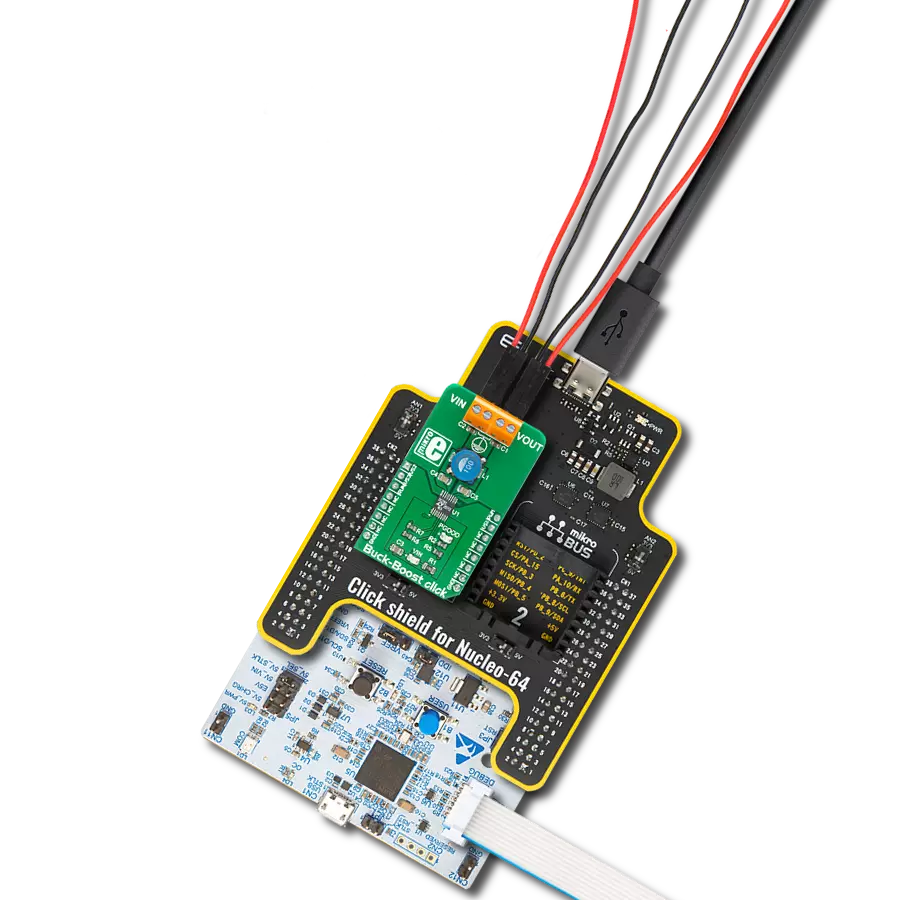
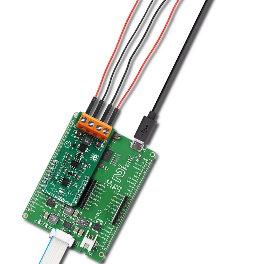
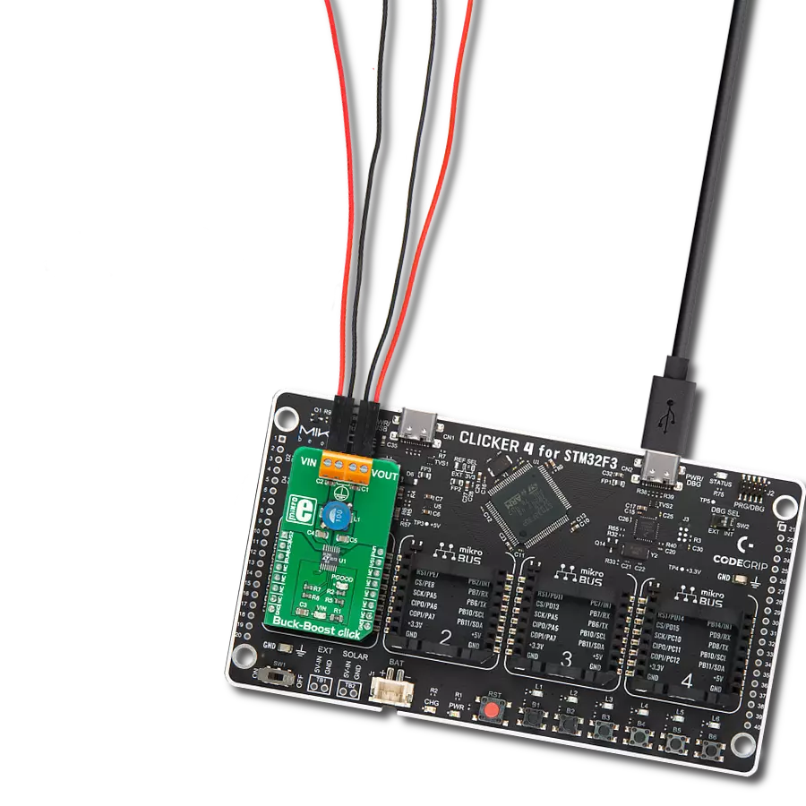
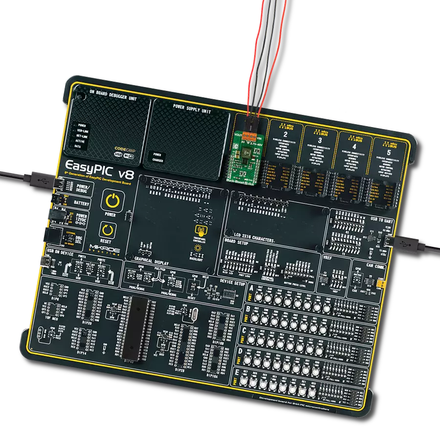
Buck-Boost 2 Click
Dev. board
Nucleo-64 with STM32F091RC MCU
Compiler
NECTO Studio
MCU
STM32F091RC
Revolutionize your energy management with our avant-garde Buck-Boost combo at your side
A
A
Hardware Overview
How does it work?
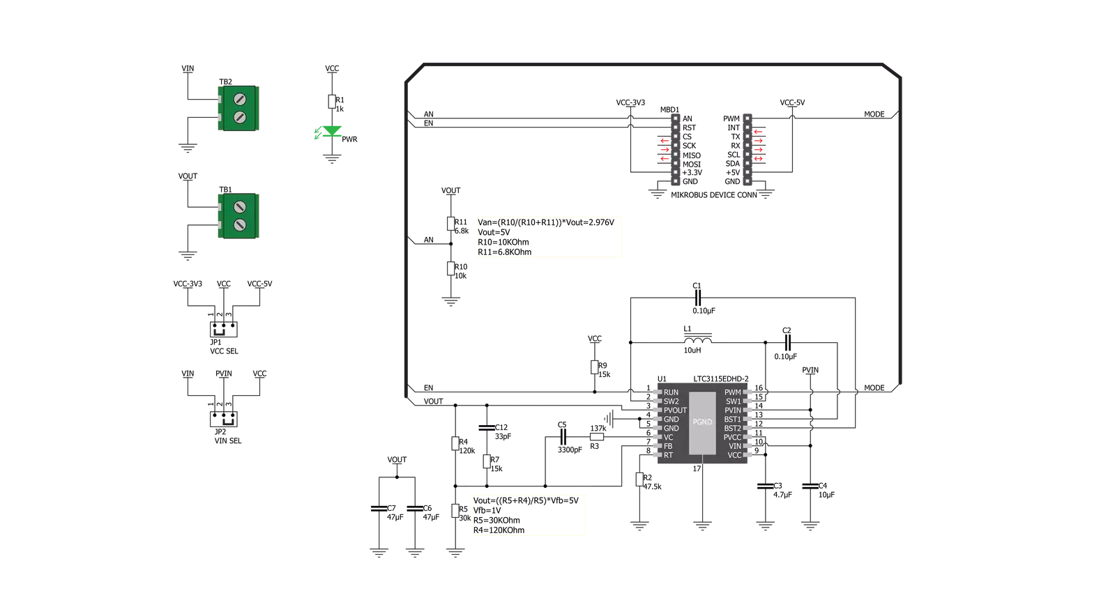
Buck-Boost 2 Click is based on the LTC3115-2, a 40V, 2A synchronous buck-boost DC/DC converter from Analog Devices. This IC relies on the advanced four MOSFET switch topology, so it can sustain the regulation when the input voltage is lower and higher than the output voltage, set by the feedback network to 5V. A proprietary switching algorithm ensures a transparent, continuous transition between operating modes. The LTC3115-2 features both forward and reverse current limiting sections. The maximum current available on the output depends on the mode of operation: If the output voltage is greater than the input voltage, the device works in boost mode, and the maximum current is about 0.6A. If the output voltage exceeds the input voltage, the device works in buck mode, and the maximum current available is about 1.4A. Also, the maximum output current is affected by the switching mode, selectable by the MODE pin, routed to the PWM pin of the mikroBUS™. There are two modes available: fixed frequency PWM mode and burst mode. While working in PWM mode, the LTC3115-2 IC uses a fixed frequency determined by the onboard resistor - in the case of the Buck-Boost 2 click, it is fixed at 750kHz. The PWM mode is used when a heavier load is connected to the output
terminal. This mode is set when the PWM/SYNC pin is pulled to a HIGH logic level. This mode allows the maximum current on the output and results in the lowest amount of switching noise and output voltage ripple. This mode provides power for the connected devices while they work in the active mode. The burst mode is used for maintained efficiency when light output loads are used. When the PWM/SYNC pin is pulled to a LOW logic level, the device will work in burst mode. While in burst mode, the variable frequency switching algorithm is used, resulting in a low quiescent current, which allows lowered power consumption - e.g., when the external voltage input is taken from a battery. The error amplifier is powered down in this mode, and the output current should not be greater than allowed, else the output voltage will lose regulation. This mode is perfectly suited to power up various devices while they work in standby mode. When using the synchronization function of the PWM/SYNC pin, the device works in the fixed frequency PWM mode, but the external clock source of the internal PLL section regulates its frequency. This can be useful when special power supply noise requirements must be met. Since the internal PLL can only increase the internal clock frequency, the
external clock signal should be above the frequency set by the onboard resistor (750kHz), taking the sufficient error margin into account. The RUN pin of the LTC3115-2 IC is routed to the mikroBUS™ RST pin and is used to activate the internal logic and switching circuitry. Setting this pin to a HIGH logic level (above 1.21V) will enable both the logic and the switching sections of the LTC3115-2 IC. It is possible to measure and monitor the output voltage of the Buck-Boost 2 by utilizing the voltage divider, with its middle point routed to the AN pin of the mikroBUS™. By applying the calculation from the formula below, it is possible to determine the exact value of the output voltage. It can monitor the output to take appropriate action when the voltage drops or loses regulation. This board allows operation with both 3.3V and 5V MCUs. There is an onboard SMD jumper labeled as VCC SEL, which is used to set the logic voltage (e.g., for the RUN pin) and the input voltage for the LTC3115-2 IC. Another SMD jumper, labeled VIN SEL, selects the voltage chosen by the VCC SEL and the external source connected to the input terminal. The output load should be connected to the output terminal. Two screw terminals allow easy and secure connection of the input and output lines.

Features overview
Development board
Nucleo-64 with STM32F091RC MCU offers a cost-effective and adaptable platform for developers to explore new ideas and prototype their designs. This board harnesses the versatility of the STM32 microcontroller, enabling users to select the optimal balance of performance and power consumption for their projects. It accommodates the STM32 microcontroller in the LQFP64 package and includes essential components such as a user LED, which doubles as an ARDUINO® signal, alongside user and reset push-buttons, and a 32.768kHz crystal oscillator for precise timing operations. Designed with expansion and flexibility in mind, the Nucleo-64 board features an ARDUINO® Uno V3 expansion connector and ST morpho extension pin
headers, granting complete access to the STM32's I/Os for comprehensive project integration. Power supply options are adaptable, supporting ST-LINK USB VBUS or external power sources, ensuring adaptability in various development environments. The board also has an on-board ST-LINK debugger/programmer with USB re-enumeration capability, simplifying the programming and debugging process. Moreover, the board is designed to simplify advanced development with its external SMPS for efficient Vcore logic supply, support for USB Device full speed or USB SNK/UFP full speed, and built-in cryptographic features, enhancing both the power efficiency and security of projects. Additional connectivity is
provided through dedicated connectors for external SMPS experimentation, a USB connector for the ST-LINK, and a MIPI® debug connector, expanding the possibilities for hardware interfacing and experimentation. Developers will find extensive support through comprehensive free software libraries and examples, courtesy of the STM32Cube MCU Package. This, combined with compatibility with a wide array of Integrated Development Environments (IDEs), including IAR Embedded Workbench®, MDK-ARM, and STM32CubeIDE, ensures a smooth and efficient development experience, allowing users to fully leverage the capabilities of the Nucleo-64 board in their projects.

Microcontroller Overview
MCU Card / MCU

Architecture
ARM Cortex-M0
MCU Memory (KB)
256
Silicon Vendor
STMicroelectronics
Pin count
64
RAM (Bytes)
32768
You complete me!
Accessories
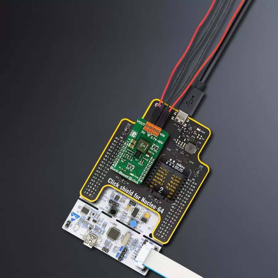
Click Shield for Nucleo-64 comes equipped with two proprietary mikroBUS™ sockets, allowing all the Click board™ devices to be interfaced with the STM32 Nucleo-64 board with no effort. This way, Mikroe allows its users to add any functionality from our ever-growing range of Click boards™, such as WiFi, GSM, GPS, Bluetooth, ZigBee, environmental sensors, LEDs, speech recognition, motor control, movement sensors, and many more. More than 1537 Click boards™, which can be stacked and integrated, are at your disposal. The STM32 Nucleo-64 boards are based on the microcontrollers in 64-pin packages, a 32-bit MCU with an ARM Cortex M4 processor operating at 84MHz, 512Kb Flash, and 96KB SRAM, divided into two regions where the top section represents the ST-Link/V2 debugger and programmer while the bottom section of the board is an actual development board. These boards are controlled and powered conveniently through a USB connection to program and efficiently debug the Nucleo-64 board out of the box, with an additional USB cable connected to the USB mini port on the board. Most of the STM32 microcontroller pins are brought to the IO pins on the left and right edge of the board, which are then connected to two existing mikroBUS™ sockets. This Click Shield also has several switches that perform functions such as selecting the logic levels of analog signals on mikroBUS™ sockets and selecting logic voltage levels of the mikroBUS™ sockets themselves. Besides, the user is offered the possibility of using any Click board™ with the help of existing bidirectional level-shifting voltage translators, regardless of whether the Click board™ operates at a 3.3V or 5V logic voltage level. Once you connect the STM32 Nucleo-64 board with our Click Shield for Nucleo-64, you can access hundreds of Click boards™, working with 3.3V or 5V logic voltage levels.

Used MCU Pins
mikroBUS™ mapper
Take a closer look
Click board™ Schematic
Step by step
Project assembly
Start by selecting your development board and Click board™. Begin with the Nucleo-64 with STM32F091RC MCU as your development board.


Track your results in real time
Application Output
1. Application Output - In Debug mode, the 'Application Output' window enables real-time data monitoring, offering direct insight into execution results. Ensure proper data display by configuring the environment correctly using the provided tutorial.

2. UART Terminal - Use the UART Terminal to monitor data transmission via a USB to UART converter, allowing direct communication between the Click board™ and your development system. Configure the baud rate and other serial settings according to your project's requirements to ensure proper functionality. For step-by-step setup instructions, refer to the provided tutorial.

3. Plot Output - The Plot feature offers a powerful way to visualize real-time sensor data, enabling trend analysis, debugging, and comparison of multiple data points. To set it up correctly, follow the provided tutorial, which includes a step-by-step example of using the Plot feature to display Click board™ readings. To use the Plot feature in your code, use the function: plot(*insert_graph_name*, variable_name);. This is a general format, and it is up to the user to replace 'insert_graph_name' with the actual graph name and 'variable_name' with the parameter to be displayed.

Software Support
Library Description
This library contains API for Buck-Boost 2 Click driver.
Key functions:
buckboost2_set_mode- This function sets the working modebuckboost2_power_off- This function powers OFF the chipbuckboost2_power_on- This function powers on the chip
Open Source
Code example
The complete application code and a ready-to-use project are available through the NECTO Studio Package Manager for direct installation in the NECTO Studio. The application code can also be found on the MIKROE GitHub account.
/*!
 * \file
 * \brief Buck Boost 2 Click example
 *
 * # Description
 * This application enables use of DC-DC step-down/step-up regulator (buck/boost).
 *
 * The demo application is composed of two sections :
 *
 * ## Application Init
 * Initializes Driver init and turn ON chip and settings mode with improvement current.
 *
 * ## Application Task
 * The Click has a constant output voltage of 5V, no additional settings are required.
 *
 *
 * \author MikroE Team
 *
 */
// ------------------------------------------------------------------- INCLUDES

#include "board.h"
#include "log.h"
#include "buckboost2.h"

// ------------------------------------------------------------------ VARIABLES

static buckboost2_t buckboost2;
static log_t logger;

// ------------------------------------------------------ APPLICATION FUNCTIONS

void application_init ( void )
{
    log_cfg_t log_cfg;
    buckboost2_cfg_t cfg;

    /**
     * Logger initialization.
     * Default baud rate: 115200
     * Default log level: LOG_LEVEL_DEBUG
     * @note If USB_UART_RX and USB_UART_TX
     * are defined as HAL_PIN_NC, you will
     * need to define them manually for log to work.
     * See @b LOG_MAP_USB_UART macro definition for detailed explanation.
     */
    LOG_MAP_USB_UART( log_cfg );
    log_init( &logger, &log_cfg );
    log_info(&logger, "---- Application Init ----");

    //  Click initialization.

    buckboost2_cfg_setup( &cfg );
    BUCKBOOST2_MAP_MIKROBUS( cfg, MIKROBUS_1 );
    buckboost2_init( &buckboost2, &cfg );

    buckboost2_power_on( &buckboost2 );
    buckboost2_set_mode( &buckboost2, BUCKBOOST2_WITH_IMPROVEMENT );
}

void application_task ( void )
{
    //  Task implementation.

}

int main ( void )
{
    /* Do not remove this line or clock might not be set correctly. */
    #ifdef PREINIT_SUPPORTED
    preinit();
    #endif

    application_init( );

    for ( ; ; )
    {
        application_task( );
    }

    return 0;
}


// ------------------------------------------------------------------------ END